
Datasheet


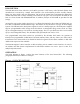
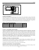
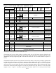
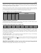
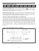
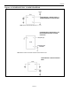
Table Of Contents
- BENEFITS AND FEATURES
- ORDERING INFORMATION
- DESCRIPTION
- Figure 1. BLOCK DIAGRAM
- CLOCK ACCURACY
- CLOCK, CALENDAR, AND ALARM
- WRITING TO THE CLOCK REGISTERS
- READING FROM THE CLOCK REGISTERS
- FUNCTION
- BIT7
- 1Hz (1Hz Output Enable) – This bit controls the 1Hz output. When this bit is a logic 1, the 1Hz output is enabled. When this bit is a logic 0, the 1Hz output is high-Z.
- AIE0 (Alarm Interrupt Enable 0) – When set to a logic 1, this bit permits the interrupt 0 request flag (IRQF0) bit in the status register to assert . When the AIE0 bit is set to logic 0, the IRQF0 bit does not initiate the signal.
- AIE1 (Alarm Interrupt Enable 1) – When set to a logic 1, this bit permits the interrupt 1 request flag (IRQF1) bit in the status register to assert INT1. When the AIE1 bit is set to logic 0, the IRQF1 bit does not initiate an interrupt signal, and the...
- STATUS REGISTER (READ 10H)
- TRICKLE CHARGE REGISTER (READ 11H, WRITE 91H)
- Table 3. TRICKLE CHARGER RESISTOR AND DIODE SELECT
- POWER CONTROL
- Figure 4. POWER-SUPPLY CONFIGURATIONS
- SERIAL INTERFACE
- SERIAL PERIPHERAL INTERFACE (SPI)
- Figure 5. SERIAL CLOCK AS A FUNCTION OF MICROCONTROLLER
- CLOCK POLARITY (CPOL)
- ADDRESS AND DATA BYTES
- Figure 6. SPI SINGLE-BYTE WRITE
- Figure 7. SPI SINGLE-BYTE READ
- Figure 8. SPI MULTIPLE-BYTE BURST TRANSFER
- BIT7
- READING AND WRITING IN BURST MODE
- Burst mode is similar to a single-byte read or write, except that CE is kept high and additional SCLK cycles are sent until the end of the burst. The clock registers and the user RAM may be read or written in burst mode. When accessing the clock regis...
- 3-WIRE INTERFACE
- Figure 9. 3-WIRE SINGLE BYTE TRANSFER
- ABSOLUTE MAXIMUM RATINGS
- RECOMMENDED DC OPERATING CONDITIONS (TA = Over the operating range, unless otherwise specified.)
- CAPACITANCE (TA = +25C)
- Figure 10. TIMING DIAGRAM: 3-WIRE READ DATA TRANSFER
- Figure 11. TIMING DIAGRAM: 3-WIRE WRITE DATA TRANSFER
- SPI AC ELECTRICAL CHARACTERISTICS (TA = Over the operating range, unless otherwise specified.)
- Figure 12. TIMING DIAGRAM: SPI READ DATA TRANSFER
- Figure 13. TIMING DIAGRAM: SPI WRITE DATA TRANSFER
- NOTES:
- REVISION HISTORY
- SYMBOL
- PARAMETER
- SYMBOL
- SYMBOL
- PARAMETER
- SYMBOL
- PARAMETER

DS1306
RECOMMENDED LAYOUT FOR CRYSTAL
CLOCK ACCURACY
The accuracy of the clock is dependent upon the accuracy of the crystal and the accuracy of the match
between the capacitive load of the oscillator circuit and the capacitive load for which the crystal was
trimmed. Additional error is added by crystal frequency drift caused by temperature shifts. External
circuit noise coupled into the oscillator circuit can result in the clock running fast. Refer to Application
Note 58: Crystal Considerations with Dallas Real-Time Clocks for detailed information.
Table 1. Crystal Specifications
PARAMETER
SYMBOL
MIN
TYP
MAX
UNITS
Nominal Frequency
f
O
32.768
kHz
Series Resistance
ESR
45
kΩ
Load Capacitance
C
L
6
pF
*The crystal, traces, and crystal input pins should be isolated from RF generating signals. Refer to
Application Note 58: Crystal Considerations for Dallas Real-Time Clocks for additional specifications.
CLOCK, CALENDAR, AND ALARM
The time and calendar information is obtained by reading the appropriate register bytes. The RTC
registers are illustrated in Figure 2. The time, calendar, and alarm are set or initialized by writing the
appropriate register bytes. Note that some bits are set to 0. These bits always read 0 regardless of how
they are written. Also note that registers 12h to 1Fh (read) and registers 92h to 9Fh are reserved. These
registers always read 0 regardless of how they are written. The contents of the time, calendar, and alarm
registers are in the BCD format.. Values in the day register that correspond to the day of the week are
user-defined, but must be sequential (e.g. if 1 equals Sunday, 2 equals Monday and so on). The day
register increments at midnight. Illogical time and date entries result in undefined operation.
WRITING TO THE CLOCK REGISTERS
The internal time and date registers continue to increment during write operations. However, the
countdown chain is reset when the seconds register is written. Writing the time and date registers within
one second after writing the seconds register ensures consistent data.
Terminating a write before the last bit is sent aborts the write for that byte.
READING FROM THE CLOCK REGISTERS
Buffers are used to copy the time and date register at the beginning of a read. When reading in burst
mode, the user copy is static while the internal registers continue to increment.
Local ground plane (Layer 2)
crystal
X1
X2
GND
5 of 22