
Datasheet


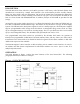
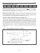
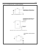
Table Of Contents
- BENEFITS AND FEATURES
- ORDERING INFORMATION
- DESCRIPTION
- Figure 1. BLOCK DIAGRAM
- CLOCK ACCURACY
- CLOCK, CALENDAR, AND ALARM
- WRITING TO THE CLOCK REGISTERS
- READING FROM THE CLOCK REGISTERS
- FUNCTION
- BIT7
- 1Hz (1Hz Output Enable) – This bit controls the 1Hz output. When this bit is a logic 1, the 1Hz output is enabled. When this bit is a logic 0, the 1Hz output is high-Z.
- AIE0 (Alarm Interrupt Enable 0) – When set to a logic 1, this bit permits the interrupt 0 request flag (IRQF0) bit in the status register to assert . When the AIE0 bit is set to logic 0, the IRQF0 bit does not initiate the signal.
- AIE1 (Alarm Interrupt Enable 1) – When set to a logic 1, this bit permits the interrupt 1 request flag (IRQF1) bit in the status register to assert INT1. When the AIE1 bit is set to logic 0, the IRQF1 bit does not initiate an interrupt signal, and the...
- STATUS REGISTER (READ 10H)
- TRICKLE CHARGE REGISTER (READ 11H, WRITE 91H)
- Table 3. TRICKLE CHARGER RESISTOR AND DIODE SELECT
- POWER CONTROL
- Figure 4. POWER-SUPPLY CONFIGURATIONS
- SERIAL INTERFACE
- SERIAL PERIPHERAL INTERFACE (SPI)
- Figure 5. SERIAL CLOCK AS A FUNCTION OF MICROCONTROLLER
- CLOCK POLARITY (CPOL)
- ADDRESS AND DATA BYTES
- Figure 6. SPI SINGLE-BYTE WRITE
- Figure 7. SPI SINGLE-BYTE READ
- Figure 8. SPI MULTIPLE-BYTE BURST TRANSFER
- BIT7
- READING AND WRITING IN BURST MODE
- Burst mode is similar to a single-byte read or write, except that CE is kept high and additional SCLK cycles are sent until the end of the burst. The clock registers and the user RAM may be read or written in burst mode. When accessing the clock regis...
- 3-WIRE INTERFACE
- Figure 9. 3-WIRE SINGLE BYTE TRANSFER
- ABSOLUTE MAXIMUM RATINGS
- RECOMMENDED DC OPERATING CONDITIONS (TA = Over the operating range, unless otherwise specified.)
- CAPACITANCE (TA = +25C)
- Figure 10. TIMING DIAGRAM: 3-WIRE READ DATA TRANSFER
- Figure 11. TIMING DIAGRAM: 3-WIRE WRITE DATA TRANSFER
- SPI AC ELECTRICAL CHARACTERISTICS (TA = Over the operating range, unless otherwise specified.)
- Figure 12. TIMING DIAGRAM: SPI READ DATA TRANSFER
- Figure 13. TIMING DIAGRAM: SPI WRITE DATA TRANSFER
- NOTES:
- REVISION HISTORY
- SYMBOL
- PARAMETER
- SYMBOL
- SYMBOL
- PARAMETER
- SYMBOL
- PARAMETER

DS1306
DESCRIPTION
The DS1306 serial alarm real-time clock (RTC) provides a full binary coded decimal (BCD) clock
calendar that is accessed by a simple serial interface. The clock/calendar provides seconds, minutes,
hours, day, date, month, and year information. The end of the month date is automatically adjusted for
months with fewer than 31 days, including corrections for leap year. The clock operates in either the 24-
hour or 12-hour format with AM/PM indicator. In addition, 96 bytes of NV RAM are provided for data
storage.
An interface logic power-supply input pin (V
CCIF
) allows the DS1306 to drive SDO and 32kHz pins to a
level that is compatible with the interface logic. This allows an easy interface to 3V logic in mixed supply
systems. The DS1306 offers dual-power supplies as well as a battery-input pin. The dual-power supplies
support a programmable trickle charge circuit that allows a rechargeable energy source (such as a super
cap or rechargeable battery) to be used for a backup supply. The V
BAT
pin allows the device to be backed
up by a non-rechargeable battery. The DS1306 is fully operational from 2.0V to 5.5V.
Two programmable time-of-day alarms are provided by the DS1306. Each alarm can generate an
interrupt on a programmable combination of seconds, minutes, hours, and day. “Don’t care” states can be
inserted into one or more fields if it is desired for them to be ignored for the alarm condition. A 1Hz and a
32kHz clock output are also available.
The DS1306 supports a direct interface to SPI serial data ports or standard 3-wire interface. An easy-to-
use address and data format is implemented in which data transfers can occur 1 byte at a time or in
multiple-byte burst mode.
OPERATION
The block diagram in Figure 1 shows the main elements of the serial alarm RTC. The following
paragraphs describe the function of each pin.
Figure 1. BLOCK DIAGRAM
1Hz
4 of 22