
Datasheet


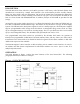
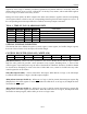
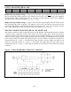
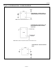
Table Of Contents
- BENEFITS AND FEATURES
- ORDERING INFORMATION
- DESCRIPTION
- Figure 1. BLOCK DIAGRAM
- CLOCK ACCURACY
- CLOCK, CALENDAR, AND ALARM
- WRITING TO THE CLOCK REGISTERS
- READING FROM THE CLOCK REGISTERS
- FUNCTION
- BIT7
- 1Hz (1Hz Output Enable) – This bit controls the 1Hz output. When this bit is a logic 1, the 1Hz output is enabled. When this bit is a logic 0, the 1Hz output is high-Z.
- AIE0 (Alarm Interrupt Enable 0) – When set to a logic 1, this bit permits the interrupt 0 request flag (IRQF0) bit in the status register to assert . When the AIE0 bit is set to logic 0, the IRQF0 bit does not initiate the signal.
- AIE1 (Alarm Interrupt Enable 1) – When set to a logic 1, this bit permits the interrupt 1 request flag (IRQF1) bit in the status register to assert INT1. When the AIE1 bit is set to logic 0, the IRQF1 bit does not initiate an interrupt signal, and the...
- STATUS REGISTER (READ 10H)
- TRICKLE CHARGE REGISTER (READ 11H, WRITE 91H)
- Table 3. TRICKLE CHARGER RESISTOR AND DIODE SELECT
- POWER CONTROL
- Figure 4. POWER-SUPPLY CONFIGURATIONS
- SERIAL INTERFACE
- SERIAL PERIPHERAL INTERFACE (SPI)
- Figure 5. SERIAL CLOCK AS A FUNCTION OF MICROCONTROLLER
- CLOCK POLARITY (CPOL)
- ADDRESS AND DATA BYTES
- Figure 6. SPI SINGLE-BYTE WRITE
- Figure 7. SPI SINGLE-BYTE READ
- Figure 8. SPI MULTIPLE-BYTE BURST TRANSFER
- BIT7
- READING AND WRITING IN BURST MODE
- Burst mode is similar to a single-byte read or write, except that CE is kept high and additional SCLK cycles are sent until the end of the burst. The clock registers and the user RAM may be read or written in burst mode. When accessing the clock regis...
- 3-WIRE INTERFACE
- Figure 9. 3-WIRE SINGLE BYTE TRANSFER
- ABSOLUTE MAXIMUM RATINGS
- RECOMMENDED DC OPERATING CONDITIONS (TA = Over the operating range, unless otherwise specified.)
- CAPACITANCE (TA = +25C)
- Figure 10. TIMING DIAGRAM: 3-WIRE READ DATA TRANSFER
- Figure 11. TIMING DIAGRAM: 3-WIRE WRITE DATA TRANSFER
- SPI AC ELECTRICAL CHARACTERISTICS (TA = Over the operating range, unless otherwise specified.)
- Figure 12. TIMING DIAGRAM: SPI READ DATA TRANSFER
- Figure 13. TIMING DIAGRAM: SPI WRITE DATA TRANSFER
- NOTES:
- REVISION HISTORY
- SYMBOL
- PARAMETER
- SYMBOL
- SYMBOL
- PARAMETER
- SYMBOL
- PARAMETER

DS1306
internally pulled low.
PIN DESCRIPTION (continued)
PIN
NAME FUNCTION
TSSOP
DIP
9 7 1Hz
1Hz Output. The 1Hz pin provides a 1Hz square wave output. This output
is active when the 1 Hz bit in the control register is a logic 1. Both INT0
and 1Hz pins are open-drain outputs. The interrupt, 1Hz signal, and the
internal clock continue to run regardless of the level of V
CC
(as long as a
power source is present).
10
8
GND
Ground
11 9 SERMODE
Serial Interface Mode. The SERMODE pin offers the flexibility to choose
between two serial interface modes. When connected to GND, standard
3-wire communication is selected. When connected to V
CC
, SPI
communication is selected.
12 10 CE
Chip Enable. The chip enable signal must be asserted high during a read or
a write for both 3-wire and SPI communication. This pin has an internal
55kΩ pulldown resistor (typical).
14 11 SCLK
Serial Clock. SCLK is used to synchronize data movement on the serial
interface for either the SPI or 3-wire interface.
15 12 SDI
Serial Data In. When SPI communication is selected, the SDI pin is the
serial data input for the SPI bus. When 3-wire communication is selected,
this pin must be tied to the SDO pin (the SDI and SDO pins function as a
single I/O pin when tied together).
16 13 SDO
Serial Data Out. When SPI communication is selected, the SDO pin is the
serial data output for the SPI bus. When 3-wire communication is selected,
this pin must be tied to the SDI pin (the SDI and SDO pins function as a
single I/O pin when tied together). V
CCIF
provides the logic-high level.
17 14 V
CCIF
Interface Logic Power-Supply Input. The V
CCIF
pin allows the DS1306 to
drive SDO and 32kHz output pins to a level that is compatible with the
interface logic, thus allowing an easy interface to 3V logic in mixed supply
systems. This pin is physically connected to the source connection of the
p-channel transistors in the output buffers of the SDO and 32kHz pins.
18 15 32kHz
32.768kHz Output. The 32kHz pin provides a 32.768kHz output. This
signal is always present. V
CCIF
provides the logic-high level.
20 16 V
CC1
Primary Power Supply. DC power is provided to the device on this pin.
V
CC1
is the primary power supply.
4, 6, 13,
19
— N.C.
No Connection
3 of 22