
Datasheet
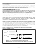
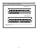
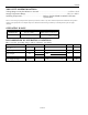
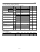
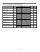
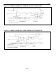
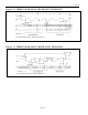
Table Of Contents
- BENEFITS AND FEATURES
- ORDERING INFORMATION
- DESCRIPTION
- Figure 1. BLOCK DIAGRAM
- CLOCK ACCURACY
- CLOCK, CALENDAR, AND ALARM
- WRITING TO THE CLOCK REGISTERS
- READING FROM THE CLOCK REGISTERS
- FUNCTION
- BIT7
- 1Hz (1Hz Output Enable) – This bit controls the 1Hz output. When this bit is a logic 1, the 1Hz output is enabled. When this bit is a logic 0, the 1Hz output is high-Z.
- AIE0 (Alarm Interrupt Enable 0) – When set to a logic 1, this bit permits the interrupt 0 request flag (IRQF0) bit in the status register to assert . When the AIE0 bit is set to logic 0, the IRQF0 bit does not initiate the signal.
- AIE1 (Alarm Interrupt Enable 1) – When set to a logic 1, this bit permits the interrupt 1 request flag (IRQF1) bit in the status register to assert INT1. When the AIE1 bit is set to logic 0, the IRQF1 bit does not initiate an interrupt signal, and the...
- STATUS REGISTER (READ 10H)
- TRICKLE CHARGE REGISTER (READ 11H, WRITE 91H)
- Table 3. TRICKLE CHARGER RESISTOR AND DIODE SELECT
- POWER CONTROL
- Figure 4. POWER-SUPPLY CONFIGURATIONS
- SERIAL INTERFACE
- SERIAL PERIPHERAL INTERFACE (SPI)
- Figure 5. SERIAL CLOCK AS A FUNCTION OF MICROCONTROLLER
- CLOCK POLARITY (CPOL)
- ADDRESS AND DATA BYTES
- Figure 6. SPI SINGLE-BYTE WRITE
- Figure 7. SPI SINGLE-BYTE READ
- Figure 8. SPI MULTIPLE-BYTE BURST TRANSFER
- BIT7
- READING AND WRITING IN BURST MODE
- Burst mode is similar to a single-byte read or write, except that CE is kept high and additional SCLK cycles are sent until the end of the burst. The clock registers and the user RAM may be read or written in burst mode. When accessing the clock regis...
- 3-WIRE INTERFACE
- Figure 9. 3-WIRE SINGLE BYTE TRANSFER
- ABSOLUTE MAXIMUM RATINGS
- RECOMMENDED DC OPERATING CONDITIONS (TA = Over the operating range, unless otherwise specified.)
- CAPACITANCE (TA = +25C)
- Figure 10. TIMING DIAGRAM: 3-WIRE READ DATA TRANSFER
- Figure 11. TIMING DIAGRAM: 3-WIRE WRITE DATA TRANSFER
- SPI AC ELECTRICAL CHARACTERISTICS (TA = Over the operating range, unless otherwise specified.)
- Figure 12. TIMING DIAGRAM: SPI READ DATA TRANSFER
- Figure 13. TIMING DIAGRAM: SPI WRITE DATA TRANSFER
- NOTES:
- REVISION HISTORY
- SYMBOL
- PARAMETER
- SYMBOL
- SYMBOL
- PARAMETER
- SYMBOL
- PARAMETER

DS1306
Figure 8. SPI MULTIPLE-BYTE BURST TRANSFER
READING AND WRITING IN BURST MODE
Burst mode is similar to a single-byte read or write, except that CE is kept high and additional SCLK
cycles are sent until the end of the burst. The clock registers and the user RAM may be read or written in
burst mode. When accessing the clock registers in burst mode, the address pointer will wrap around after
reaching 1Fh (9Fh for writes). When accessing the user RAM in burst mode, the address pointer wraps
around after reaching 7Fh (FFh for writes).
3-WIRE INTERFACE
The 3-wire interface mode operates similar to the SPI mode. However, in 3-wire mode there is one I/O
instead of separate data in and data out signals. The 3-wire interface consists of the I/O (SDI and SDO
pins tied together), CE, and SCLK pins. In 3-wire mode, each byte is shifted in LSB first, unlike SPI
mode, where each byte is shifted in MSB first.
As is the case with the SPI mode, an address byte is written to the device followed by a single data byte
or multiple data bytes. Figure 9 illustrates a read and write cycle. In 3-wire mode, data is input on the
rising edge of SCLK and output on the falling edge of SCLK.
13 of 22