
Datasheet
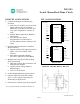


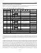
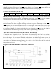
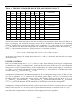
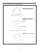
Table Of Contents
- BENEFITS AND FEATURES
- PIN CONFIGURATIONS
- ORDERING INFORMATION
- DESCRIPTION
- PIN DESCRIPTION
- OPERATION
- READING FROM THE CLOCK REGISTERS
- SPECIAL PURPOSE REGISTERS
- CONTROL REGISTER (READ 0Fh, WRITE 8Fh)
- TRICKLE CHARGE REGISTER (READ 11H, WRITE 91H)
- Figure 3. PROGRAMMABLE TRICKLE CHARGER
- POWER CONTROL
- Figure 4. POWER-SUPPLY CONFIGURATIONS
- SERIAL PERIPHERAL INTERFACE (SPI)
- ADDRESS AND DATA BYTES
- Figure 6. SPI SINGLE-BYTE WRITE
- Figure 7. SPI SINGLE-BYTE READ
- Figure 8. SPI MULTIPLE-BYTE BURST TRANSFER
- FUNCTION
- READING AND WRITING IN BURST MODE
- OPERATING RANGE
- RECOMMENDED DC OPERATING CONDITIONS (Over the operating range, unless otherwise specified.)
- DC ELECTRICAL CHARACTERISTICS (Over the operating range, unless otherwise specified.)
- CAPACITANCE (TA = +25C)
- Figure 10. TIMING DIAGRAM: 3-WIRE READ DATA TRANSFER
- SPI AC ELECTRICAL CHARACTERISTICS (Over the operating range, unless otherwise specified.) (Figure 12 and Figure 13)
- Figure 13. TIMING DIAGRAM: SPI WRITE DATA TRANSFER
- NOTES:
- REVISION HISTORY

DS1305
hour, and minute alarm registers is set to a logic 1. When bit 7 of the day, hour, minute, and seconds
alarm registers is set to a logic 1, alarm occurs every second.
During each clock update, the RTC compares the Alarm 0 and Alarm 1 registers with the corresponding
clock registers. When a match occurs, the corresponding alarm flag bit in the status register is set to a 1. If
the corresponding alarm interrupt enable bit is enabled, an interrupt output is activated.
Table 2. TIME-OF-DAY ALARM MASK BITS
ALARM REGISTER MASK BITS (BIT 7)
FUNCTION
SECONDS
MINUTES
HOURS
DAYS
1
1
1
1
Alarm once per second
0
1
1
1
Alarm when seconds match
0
0
1
1
Alarm when minutes and seconds match
0
0
0
1
Alarm hours, minutes, and seconds match
0
0
0
0
Alarm day, hours, minutes and seconds match
SPECIAL PURPOSE REGISTERS
The DS1305 has three additional registers (control register, status register, and trickle charger register)
that control the RTC, interrupts, and trickle charger.
CONTROL REGISTER (READ 0Fh, WRITE 8Fh)
BIT7
BIT6
BIT5
BIT4
BIT3
BIT2
BIT1
BIT0
EOSC
WP 0 0 0 INTCN AIE1 AIEO
EOSC
(Enable Oscillator) – This bit when set to logic 0 starts the oscillator. When this bit is set to a
logic 1, the oscillator is stopped and the DS1305 is placed into a low-power standby mode with a current
drain of less than 100nA when power is supplied by V
BAT
or V
CC2
. On initial application of power, this bit
will be set to a logic 1.
WP (Write Protect) – Before any write operation to the clock or RAM, this bit must be logic 0. When
high, the write protect bit prevents a write operation to any register, including bits 0, 1, 2, and 7 of the
control register. Upon initial power-up, the state of the WP bit is undefined. Therefore, the WP bit should
be cleared before attempting to write to the device.
INTCN (Interrupt Control) – This bit controls the relationship between the two time-of-day alarms and
the interrupt output pins. When the INTCN bit is set to a logic 1, a match between the timekeeping
registers and the Alarm 0 registers activates the
INT0
pin (provided that the alarm is enabled) and a
match between the timekeeping registers and the Alarm 1 registers activate the
INT1
pin (provided that
the alarm is enabled). When the INTCN bit is set to a logic 0, a match between the timekeeping registers
and either Alarm 0 or Alarm 1 activate the
INT0
pin (provided that the alarms are enabled).
INT1
has no
function when INTCN is set to a logic 0.
AIE0 (Alarm Interrupt Enable 0) – When set to a logic 1, this bit permits the interrupt 0 request flag
(IRQF0) bit in the status register to assert
INT0
. When the AIE0 bit is set to logic 0, the IRQF0 bit does
not initiate the
INT0
signal.
7 of 22