
Datasheet
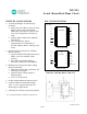


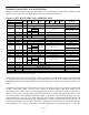
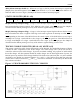
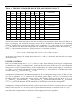
Table Of Contents
- BENEFITS AND FEATURES
- PIN CONFIGURATIONS
- ORDERING INFORMATION
- DESCRIPTION
- PIN DESCRIPTION
- OPERATION
- READING FROM THE CLOCK REGISTERS
- SPECIAL PURPOSE REGISTERS
- CONTROL REGISTER (READ 0Fh, WRITE 8Fh)
- TRICKLE CHARGE REGISTER (READ 11H, WRITE 91H)
- Figure 3. PROGRAMMABLE TRICKLE CHARGER
- POWER CONTROL
- Figure 4. POWER-SUPPLY CONFIGURATIONS
- SERIAL PERIPHERAL INTERFACE (SPI)
- ADDRESS AND DATA BYTES
- Figure 6. SPI SINGLE-BYTE WRITE
- Figure 7. SPI SINGLE-BYTE READ
- Figure 8. SPI MULTIPLE-BYTE BURST TRANSFER
- FUNCTION
- READING AND WRITING IN BURST MODE
- OPERATING RANGE
- RECOMMENDED DC OPERATING CONDITIONS (Over the operating range, unless otherwise specified.)
- DC ELECTRICAL CHARACTERISTICS (Over the operating range, unless otherwise specified.)
- CAPACITANCE (TA = +25C)
- Figure 10. TIMING DIAGRAM: 3-WIRE READ DATA TRANSFER
- SPI AC ELECTRICAL CHARACTERISTICS (Over the operating range, unless otherwise specified.) (Figure 12 and Figure 13)
- Figure 13. TIMING DIAGRAM: SPI WRITE DATA TRANSFER
- NOTES:
- REVISION HISTORY

DS1305
READING FROM THE CLOCK REGISTERS
Buffers are used to copy the time and date register at the beginning of a read. When reading in burst
mode, the user copy is static while the internal registers continue to increment.
Figure 2. RTC REGISTERS AND ADDRESS MAP
HEX ADDRESS
Bit7 Bit6 Bit5 Bit4 Bit3 Bit2 Bit1 Bit0 RANGE
READ
WRITE
00h
80h
0
10 Seconds
Seconds
00–59
01h
81h
0
10 Minutes
Minutes
00–59
02h 82h 0
12
P
10 Hour Hours
01–12 + P/A
A
00–23
24
10
03h
83h
0
0
0
0
Day
1–7
04h
84h
0
0
10 Date
Date
1–31
05h
85h
0
0
10 Month
Month
01–12
06h
86h
10 Year
Year
00–99
—
—
Alarm 0
—
07h
87h
M
10 Seconds Alarm
Seconds Alarm
00–59
08h
88h
M
10 Minutes Alarm
Minutes Alarm
00–59
09h 89h M
12
P
10 Hour Hour Alarm
01–12 + P/A
A
24
10
00–23
0Ah
8Ah
M
0
0
0
Day Alarm
01–07
—
—
Alarm 1
—
0Bh
8Bh
M
10 Seconds Alarm
Seconds Alarm
00–59
0Ch
8Ch
M
10 Minutes Alarm
Minutes Alarm
00–59
0Dh 8Dh M
12
P
10 Hour Hour Alarm
01–12 + P/A
A
24
10
00–23
0Eh
8Eh
M
0
0
0
Day Alarm
01–07
0Fh
8Fh
Control Register
—
10h
90h
Status Register
—
11h
91h
Trickle Charger Register
—
12h–1Fh
92h–9Fh
Reserved
—
20h–7Fh
A0h–FFh
96 Bytes User RAM
00–FF
Note: Range for alarm registers does not include mask’m’ bits.
The DS1305 can be run in either 12-hour or 24-hour mode. Bit 6 of the hours register is defined as the
12- or 24-hour mode select bit. When high, the 12-hour mode is selected. In the 12-hour mode, bit 5 is the
AM/PM bit with logic high being PM. In the 24-hour mode, bit 5 is the second 10-hour bit (20 to 23
hours).
The DS1305 contains two time-of-day alarms. Time-of-day Alarm 0 can be set by writing to registers 87h
to 8Ah. Time-of-day Alarm 1 can be set by writing to registers 8Bh to 8Eh. The alarms can be
programmed (by the INTCN bit of the control register) to operate in two different modes; each alarm can
drive its own separate interrupt output or both alarms can drive a common interrupt output. Bit 7 of each
of the time-of-day alarm registers are mask bits (Table 2). When all of the mask bits are logic 0, a time-
of-day alarm only occurs once per week when the values stored in timekeeping registers 00h to 03h
match the values stored in the time-of-day alarm registers. An alarm is generated every day when bit 7 of
the day alarm register is set to a logic 1. An alarm is generated every hour when bit 7 of the day and hour
alarm registers is set to a logic 1. Similarly, an alarm is generated every minute when bit 7 of the day,
6 of 22