
Datasheet


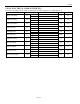

Table Of Contents
- BENEFITS AND FEATURES
- PIN CONFIGURATIONS
- ORDERING INFORMATION
- DESCRIPTION
- PIN DESCRIPTION
- OPERATION
- READING FROM THE CLOCK REGISTERS
- SPECIAL PURPOSE REGISTERS
- CONTROL REGISTER (READ 0Fh, WRITE 8Fh)
- TRICKLE CHARGE REGISTER (READ 11H, WRITE 91H)
- Figure 3. PROGRAMMABLE TRICKLE CHARGER
- POWER CONTROL
- Figure 4. POWER-SUPPLY CONFIGURATIONS
- SERIAL PERIPHERAL INTERFACE (SPI)
- ADDRESS AND DATA BYTES
- Figure 6. SPI SINGLE-BYTE WRITE
- Figure 7. SPI SINGLE-BYTE READ
- Figure 8. SPI MULTIPLE-BYTE BURST TRANSFER
- FUNCTION
- READING AND WRITING IN BURST MODE
- OPERATING RANGE
- RECOMMENDED DC OPERATING CONDITIONS (Over the operating range, unless otherwise specified.)
- DC ELECTRICAL CHARACTERISTICS (Over the operating range, unless otherwise specified.)
- CAPACITANCE (TA = +25C)
- Figure 10. TIMING DIAGRAM: 3-WIRE READ DATA TRANSFER
- SPI AC ELECTRICAL CHARACTERISTICS (Over the operating range, unless otherwise specified.) (Figure 12 and Figure 13)
- Figure 13. TIMING DIAGRAM: SPI WRITE DATA TRANSFER
- NOTES:
- REVISION HISTORY

DS1305
REVISION HISTORY
REVISION
DATE
DESCRIPTION
PAGES
CHANGED
12/09
Added Table 1. Crystal Specifications to the Clock Accuracy section. 5
Added “SERMODE = V
CC
” to Figures 6, 7, 12, and 13. 12, 20
Added “SERMODE = GND” to Figures 9, 10, and 11. 14, 18
Removed the “Crystal Capacitance” parameter from the Capacitance
table.
16
4/15 Revised Benefits and Features section 1
Maxim cannot assume responsibility for use of any circuitry other than circuitry entirely embodied in a Maxim product. No circuit patent licenses are implied. Maxim
reserves the right to change the circuitry and specifications without notice at any time.
Maxim Integrated Products, 160 Rio Robles, San Jose, CA 95134 408-601-1000
© 2015 Maxim Integrated Products Maxim is a registered trademark of Maxim Integrated Products, Inc.
22 of 22