
Datasheet
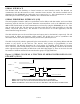


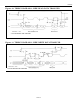

Table Of Contents
- BENEFITS AND FEATURES
- PIN CONFIGURATIONS
- ORDERING INFORMATION
- DESCRIPTION
- PIN DESCRIPTION
- OPERATION
- READING FROM THE CLOCK REGISTERS
- SPECIAL PURPOSE REGISTERS
- CONTROL REGISTER (READ 0Fh, WRITE 8Fh)
- TRICKLE CHARGE REGISTER (READ 11H, WRITE 91H)
- Figure 3. PROGRAMMABLE TRICKLE CHARGER
- POWER CONTROL
- Figure 4. POWER-SUPPLY CONFIGURATIONS
- SERIAL PERIPHERAL INTERFACE (SPI)
- ADDRESS AND DATA BYTES
- Figure 6. SPI SINGLE-BYTE WRITE
- Figure 7. SPI SINGLE-BYTE READ
- Figure 8. SPI MULTIPLE-BYTE BURST TRANSFER
- FUNCTION
- READING AND WRITING IN BURST MODE
- OPERATING RANGE
- RECOMMENDED DC OPERATING CONDITIONS (Over the operating range, unless otherwise specified.)
- DC ELECTRICAL CHARACTERISTICS (Over the operating range, unless otherwise specified.)
- CAPACITANCE (TA = +25C)
- Figure 10. TIMING DIAGRAM: 3-WIRE READ DATA TRANSFER
- SPI AC ELECTRICAL CHARACTERISTICS (Over the operating range, unless otherwise specified.) (Figure 12 and Figure 13)
- Figure 13. TIMING DIAGRAM: SPI WRITE DATA TRANSFER
- NOTES:
- REVISION HISTORY

DS1305
Figure 8. SPI MULTIPLE-BYTE BURST TRANSFER
READING AND WRITING IN BURST MODE
Burst mode is similar to a single-byte read or write, except that CE is kept high and additional SCLK
cycles are sent until the end of the burst. The clock registers and the user RAM can be read or written in
burst mode. When accessing the clock registers in burst mode, the address pointer wraps around after
reaching 1Fh (9Fh for writes). When accessing the user RAM in burst mode, the address pointer wraps
around after reaching 7Fh (FFh for writes).
13 of 22