
Datasheet
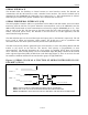


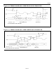

Table Of Contents
- BENEFITS AND FEATURES
- PIN CONFIGURATIONS
- ORDERING INFORMATION
- DESCRIPTION
- PIN DESCRIPTION
- OPERATION
- READING FROM THE CLOCK REGISTERS
- SPECIAL PURPOSE REGISTERS
- CONTROL REGISTER (READ 0Fh, WRITE 8Fh)
- TRICKLE CHARGE REGISTER (READ 11H, WRITE 91H)
- Figure 3. PROGRAMMABLE TRICKLE CHARGER
- POWER CONTROL
- Figure 4. POWER-SUPPLY CONFIGURATIONS
- SERIAL PERIPHERAL INTERFACE (SPI)
- ADDRESS AND DATA BYTES
- Figure 6. SPI SINGLE-BYTE WRITE
- Figure 7. SPI SINGLE-BYTE READ
- Figure 8. SPI MULTIPLE-BYTE BURST TRANSFER
- FUNCTION
- READING AND WRITING IN BURST MODE
- OPERATING RANGE
- RECOMMENDED DC OPERATING CONDITIONS (Over the operating range, unless otherwise specified.)
- DC ELECTRICAL CHARACTERISTICS (Over the operating range, unless otherwise specified.)
- CAPACITANCE (TA = +25C)
- Figure 10. TIMING DIAGRAM: 3-WIRE READ DATA TRANSFER
- SPI AC ELECTRICAL CHARACTERISTICS (Over the operating range, unless otherwise specified.) (Figure 12 and Figure 13)
- Figure 13. TIMING DIAGRAM: SPI WRITE DATA TRANSFER
- NOTES:
- REVISION HISTORY

DS1305
* SCLK CAN BE EITHER POLARITY.
ADDRESS AND DATA BYTES
Address and data bytes are shifted MSB first into the serial data input (SDI) and out of the serial data
output (SDO). Any transfer requires the address of the byte to specify a write or read to either a RTC or
RAM location, followed by one or more bytes of data. Data is transferred out of the SDO for a read
operation and into the SDI for a write operation (Figures 6 and 7).
Figure 6. SPI SINGLE-BYTE WRITE
Figure 7. SPI SINGLE-BYTE READ
The address byte is always the first byte entered after CE is driven high. The most significant bit (A7) of
this byte determines if a read or write takes place. If A7 is 0, one or more read cycles occur. If A7 is 1,
one or more write cycles occur.
Data transfers can occur one byte at a time or in multiple-byte burst mode. After CE is driven high an
address is written to the DS1305. After the address, one or more data bytes can be written or read. For a
single-byte transfer, one byte is read or written and then CE is driven low. For a multiple-byte transfer,
however, multiple bytes can be read or written to the DS1305 after the address has been written. Each
read or write cycle causes the RTC register or RAM address to automatically increment. Incrementing
continues until the device is disabled. When the RTC is selected, the address wraps to 00h after
incrementing to 1Fh (during a read) and wraps to 80h after incrementing to 9Fh (during a write). When
the RAM is selected, the address wraps to 20h after incrementing to 7Fh (during a read) and wraps to
A0h after incrementing to FFh (during a write).
* SCLK CAN BE EITHER POLARITY.
SERMODE = V
CC
SERMODE = V
CC
12 of 22