
Datasheet


DS1305
4 of 22
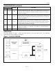
PIN DESCRIPTION (continued)
PIN
DIP TSSOP
NAME
FUNCTION
12 15 SDI
Serial Data Input. When SPI communication is selected, the SDI pin is the
serial data input for the SPI bus. When 3-wire communication is selected, this
pin must be tied to the SDO pin (the SDI and SDO pins function as a single I/O
pin when tied together).
13 16 SDO
Serial Data Output. When SPI communication is selected, the SDO pin is the
serial data output for the SPI bus. When 3-wire communication is selected, this
pin must be tied to the SDI pin (the SDI and SDO pins function as a single I/O
pin when tied together).
14 17 V
CCIF
Interface Logic Power-Supply Input. The V
CCIF
pin allows the DS1305 to drive
SDO and PF output pins to a level that is compatible with the interface logic,
thus allowing an easy interface to 3V logic in mixed supply systems. This pin is
physically connected to the source connection of the p-channel transistors in
the output buffers of the SDO and PF pins.
15 18
PF
Active-Low Power-Fail Output. The PF pin is used to indicate loss of the
primary power supply (V
CC1
). When V
CC1
is less than V
CC2
or is less than V
BAT
,
the PF pin is driven low.
16 20 V
CC1
Primary Power Supply. DC power is provided to the device on this pin.
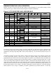
OPERATION
The block diagram in Figure 1 shows the main elements of the serial alarm RTC. The following
paragraphs describe the function of each pin.
Figure 1. BLOCK DIAGRAM
1Hz
OSCILLATOR AND
COUNTDOWN CHAIN