
Datasheet


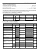
Table Of Contents
- DS1302
- Trickle-Charge Timekeeping Chip
- TYPICAL OPERATING CHARACTERISTICS
- PIN DESCRIPTION
- DATA INPUT
- DATA OUTPUT
- BURST MODE
- CLOCK/CALENDAR
- CLOCK HALT FLAG
- WRITE-PROTECT BIT
- TRICKLE-CHARGE REGISTER
- RAM
- RAM BURST MODE
- REGISTER SUMMARY
- CRYSTAL SELECTION
- CLOCK BURST
- RAM BURST
- V
- CAPACITANCE
- AC ELECTRICAL CHARACTERISTICS
- tCDH

DS1302 Trickle-Charge Timekeeping Chip
ABSOLUTE MAXIMUM RATINGS
Voltage Range on Any Pin Relative to Ground……………………………………………………………….-0.5Vto +7.0V
Operating Temperature Range, Commercial………………………………………………………………….0°C to +70°C
Operating Temperature Range, Industrial (IND)……………………………………………………………-40°C to +85°C
Storage Temperature Range……………………………………………………………………………..….-55°C to +125°C
Soldering Temperature (leads, 10 seconds)………………………………………………………………..………….260°C
Soldering Temperature (surface mount)………………………………………………..…….See IPC/JEDEC J-STD-020
Stresses beyond those listed under “Absolute Maximum Ratings” may cause permanent damage to the device. These are stress ratings only,
and functional operation of the device at these or any other conditions beyond those indicated in the operational sections of the specifications is
not implied. Exposure to the absolute maximum rating conditions for extended periods may affect device reliability.
RECOMMENDED DC OPERATING CONDITIONS
(T
A
= 0°C to +70°C or T
A
= -40°C to +85°C.) (Note 1)
PARAMETER SYMBOL CONDITIONS MIN TYP MAX UNITS
Supply Voltage V
CC1
, V
CC2
V
CC1,
V
CC2
(Notes 2, 10) 2.0 3.3 5.5 V
Logic 1 Input V
IH
(Note 2) 2.0
V
CC
+
0.3
V
Logic 0 Input V
IL
V
CC
= 2.0V
(Note 2)
-0.3 +0.3
V
V
CC
= 5V
-0.3
+0.8
DC ELECTRICAL CHARACTERISTICS
(T
A
= 0°C to +70°C or T
A
= -40°C to +85°C.) (Note 1)
PARAMETER SYMBOL CONDITIONS MIN TYP MAX UNITS
Input Leakage I
LI
(Notes 5, 13) 85 500
µA
I/O Leakage I
LO
(Notes 5, 13) 85 500
µA
Logic 1 Output (I
OH
= -0.4mA)
V
OH
V
CC
= 2.0V
(Note 2)
1.6
V
Logic 1 Output (I
OH
= -1.0mA)
V
CC
= 5V
2.4
Logic 0 Output (I
OL
= 1.5mA)
V
OL
V
CC
= 2.0V
(Note 2)
0.4
V
Logic 0 Output (I
OL
= 4.0mA)
V
CC
= 5V
0.4
Active Supply Current
(Oscillator Enabled)
I
CC1A
V
CC1
= 2.0V
CH = 0
(Notes 4, 11)
0.4
mA
V
CC1
= 5V
1.2
Timekeeping Current
(Oscillator Enabled)
I
CC1T
V
CC1
= 2.0V
CH = 0
(Notes 3, 11,13)
0.2
0.3
µA
V
CC1
= 5V
0.45
1
Standby Current (Oscillator
Disabled)
I
CC1S
V
CC1
= 2.0V
CH = 1
(Notes 9, 11, 13)
1
100
nA
V
CC1
= 5V
1
100
IND
5
200
Active Supply Current
(Oscillator Enabled)
I
CC2A
V
CC2
= 2.0V
CH = 0
(Notes 4, 12)
0.425
mA
V
CC2
= 5V
1.28
Timekeeping Current
(Oscillator Enabled)
I
CC2T
V
CC2
= 2.0V
CH = 0
(Notes 3, 12)
25.3
µA
V
CC2
= 5V
81
Standby Current (Oscillator
Disabled)
I
CC2S
V
CC2
= 2.0V
CH = 1
(Notes 9, 12)
25
µA
V
CC2
= 5V
80
Trickle-Charge Resistors
R1
2
kΩ
R2
4
R3
8
Trickle-Charge Diode Voltage
Drop
V
TD
0.7 V
10 of 13