
Datasheet


DS1251/DS1251P
5 of 20
from the timekeeping registers can proceed. The next 64 cycles will cause the phantom clock to either
receive or transmit data on DQ0, depending on the level of the
OE
pin or the
WE
pin. Cycles to other
locations outside the memory block can be interleaved with
CE
cycles without interrupting the pattern
recognition sequence or data transfer sequence to the phantom clock.
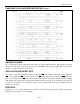
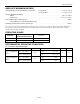
PHANTOM CLOCK REGISTER INFORMATION
The phantom clock information is contained in eight registers of 8 bits, each of which is sequentially
accessed 1 bit at a time after the 64-bit pattern recognition sequence has been completed. When updating
the phantom clock registers, each register must be handled in groups of 8 bits. Writing and reading
individual bits within a register could produce erroneous results. These read/write registers are defined in
Figure 2.
Data contained in the phantom clock register is in binary-coded decimal format (BCD). Reading and
writing the registers is always accomplished by stepping through all eight registers, starting with bit 0 of
register 0 and ending with bit 7 of register 7.
PHANTOM CLOCK REGISTER DEFINITION Figure 1
NOTE: THE PATTERN RECOGNITION IN HEX IS C5, 3A, A3, 5C, C5, 3A, A3, 5C. THE ODDS OF THIS PATTERN BEING ACCIDENTALLY
DUPLICATED AND CAUSING INADVERTENT ENTRY TO THE PHANTOM CLOCK IS LESS THAN 1 IN 10
19
. THIS PATTERN IS SENT TO
THE PHANTOM CLOCK LSB TO MSB.