
Getting Started Guide for LX9 and Nexys3 User Manual

Analog Essentials
Getting Started Guide
3
For LX9 and Nexys-3
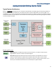
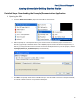
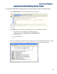
Typical System Architecture
Below is a generalized block diagram for the architecture implemented in the FPGA project. One of the key elements is
the logic block that drives each Pmod port. Each Pmod port driver contains a dedicated I
2
C port, SPI port, UART, and
octal GPIO port. Any of these can be quickly connected to the Pmod port via software control. (The multiplexer setting is
controlled by another internal GPIO port.) This eliminates the need to reprogram the FPGA during testing and evaluation
of various peripheral modules.
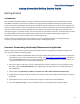
Board specific notes
Digilent Nexys-3: This FPGA board contains 4 Pmod connectors, all of which are driven by the
logic/hardware resources as shown in the above diagram.
Avnet LX9: Although the LX9 board contains 2 Pmod connectors, the FPGA does not contain a
sufficient number of gates to implement two complete copies of the drivers as shown above.
Therefore, only one of the Pmod ports on the LX9 (“J5”) is driven as shown. Pmod connector “J4” is
driven by an octal GPIO interface block and not utilized by the supplied software.