
Design Guidelines Instruction Manual

78M6610+PSU Hardware Design Guidelines AN_6610_107
18 Rev 0
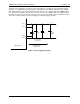
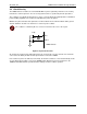
5.6 V
3P3
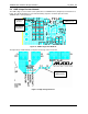
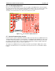
Decoupling Capacitors
Place the V
3P3
decoupling capacitors close to the 3.3V regulator and 78M6610+PSU. Provide adequate
V
3P3
copper plane from the voltage regulator and decoupling capacitors to the V
3P3D
and V
3P3D
pins of the
78M6610+PSU. Two separate V3P3A and V3P3D planes are recommended, but they should be
electrically connected via either a zero ohm resistor or inductor if needed.
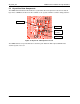
Figure 15: V
3P3
C3, C4, C5 Decoupling Capacitors
5.7 Systems Communication Interface
In most cases, the systems communication interface (UART, SPI, I
2
C) between the 78M6610+PSU and
external circuitry must be isolated to accommodate the -3.3V disparity in their GND pins (or, in the event
of a LINE reversal). Depending on various requirements, a minimum clearance barrier must exist under
the isolating components. A gap of 3 mm is the minimum requirement. Verify the isolating component’s
maximum barrier voltage meets your system requirements.
The supply for the 78M6610+PSU power domain should allow for powering the digital isolators. A low
baud rate serial UART interface is recommended for lowest power and cost associated with the digital
isolation.