
Specifications


5 CAN I/O Support for FIFO
5-26
information is provided by a row vector with 4 elements, where the first two are
used to define the acceptance mask and acceptance code for Standard
identifiers and the latter two for Extended identifiers. The default value
defined by the Setup block doesn’t filter out any messages. For information how
to define the acceptance information in order to filter certain messages, see See
“Acceptance Filters” on page 5-38.
Enable error frame detection — Defines if the CAN controller should detect
Error frames and forward these to the Receive FIFO. Checking this box makes
sense for monitoring applications where you want to be informed about all
events going over the bus. For low latency time applications, checking this box
may increase the FIFO Read driver block latency because the receive FIFO
gets filled with additional events.
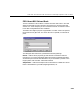
Initialization (struct) and Termination (struct) — Define CAN messages
sent during initialization and termination of the Setup block. For more
information, see Chapter 4, “CAN I/O Support”.
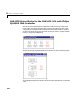
I/O Base address — Defines the I/O base address of the board to be accessed
by this block instance. The I/O base address is given by the DIP-switch setting
on the board itself. The I/O address range is 3 bytes and is mainly used to
transfer the information which memory base address the board should use. See
the Softing user manual for this board on how the I/O base address can be set.
The I/O base address entered in this control has to correspond with the
DIP-switch setting on the board. If more than one board is present in the target
system a different I/O base address has to be entered for each board. In this
case the I/O base address itself defines which board is referenced by which
board number.
Memory base address — Defines the memory base address of the board to be
accessed by this block instance. The memory base address is a software setting
only (no corresponding DIP-switch is found on the board). The memory address
range is 64k bytes. If more than one board is present in the target system a
different memory base address has to be entered for each board and you have
to make sure that the defined address ranges do not overlap. Because the xPC
Target kernel only reserves a subset of the address range between 640k bytes
and 1M bytes for memory mapped devices the address ranges have to lie within
the following range:
C0000 – DC000