Industrial Electrical Engineering and Automation CODEN:LUTEDX/(TEIE-5259)/1-57/(2008) Evaluation of a DSP for power electronic applications Per Molin Dept.
Evaluation of a DSP for power electronic applications Master Thesis work, 2008 at The Department of Industrial Electrical Engineering and Automation, LTH Per Molin, E-01
Acknowledgements The author would like to thank Magnus Akke and Gunnar Lindstedt for their invaluable support and expertise during this project.
Table of contents TABLE OF CONTENTS...................................................................................................................... 2 1 - INTRODUCTION AND PROJECT OUTLINE ........................................................................... 4 1.1 - OUTLINE OF THE REPORT .............................................................................................................. 4 2 - ALTERNATIVES AND THEIR PROPERTIES ..............................................................
A.3 - HARDWARE .................................................................................................................................. 21 A.3.1 – THE LEDS ................................................................................................................................. 22 A.3.2 – THE BUTTONS ............................................................................................................................ 23 A.3.3 – ANALOG INPUTS AND ADC....................................
1 - Introduction and project outline The complexity of the power grid increases with its continuous expansion and the addition of software controlled applications. These applications can be found in both loads and generators – as well as surveillance units. In most cases strict demands regarding performance and speed has to be fulfilled by the control scripts of these software applications.
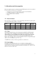
2 - Alternatives and their properties Before choosing the system to be evaluated, four main DSP-alternatives have been scrutinized in order to find the one that best fits our requirements: • • • • eZdsp F2812 from Spectrum Digital (DSP controller by Texas Instruments) LabVIEW and hardware from National Instruments PC with APCI-3110 from Addi-Data DSpace 2.1 – Areas of interest Each system has its own advantages, as well as disadvantages.
2.1.3 - Signal levels Regarding signal levels, the eZdsp is the only alternative that doesn’t support the standardized [-10, 10] V by default – however, as part of a previous master thesis, a custom built interface card has been fitted to the system in order to receive proper signal levels. 2.1.4 - Ethernet Network connectivity is not of any main concern, though it is a nice feature mastered by National Instruments.
3 - Hardware In the previous chapter the decision to evaluate the Spectrum Digital eZdsp F2812 was made. The obvious reasons for choosing the eZdsp is the price and versatile nature of the chip, should one like to mass produce a product – the DSP-chip from Texas Instruments is available at a cost that none of the alternatives can hope to rival. Another reason for choosing this development board is that MATLAB/Simulink has specific software tools for programming it.
Each event manager is equipped with two independent timers – making it a total of four. Timers are useful when handling time critical algorithms or adding delays. The timer works more or less like an “egg clock”, where the timer counts either up or down with a 16-bit value (which can be defined by the user) and causes an interrupt at a user-specified value. Also available to each event manager is eight PWM waveforms.
4 - Software A number of software tools has been used and evaluated for this report, giving the user two main alternatives when programming – either using Code Composer Studio (CCS) for traditional coding, or modeling in Simulink. The specific programs and plugins used are: Code Composer Studio v3.1 MATLAB R2007a Simulink v6.6 Embedded IDE Link CC v3.
Screenshot of CCS 3.1 CCS v3.1 comes with a selection of emulators, including a F2812 specific. This is a great feature considering that the hardware may not always be available. The emulators allow you to build and even run your programs, though without the features provided by the hardware such as PWM and ADC. The Target Support Package and Embedded IDE Link contain Simulink blocks for hardware setup and hardware specific functions respectively.
5 - Implementation of a digital relaying algorithm 5.1 – Relays of the past and present Since the beginning of the 20th century, relays built with electromechanical components have been used. Reliability and robustness are characteristics for these power electronic artifacts, and have contributed to their long reign of success. In the 1960’s, the first investigations into computer relaying was made. The idea at the time was to integrate all relay applications in one substation into a single computer.
5.2 – The model To check the suitability of the DSP regarding power electronic applications, a simplified relay model is constructed. The model contains two DFT-algorithms for signal analysis which is sufficient for detecting both phase anomalies and amplitude changes. The model of the implemented relay A more detailed view of the model as well as the generated C-code can be found in appendixes D and E.
6 - Benchmark Considering that relays and circuit breakers demand short response times between the actual error and the moment when the signal has been analysed, a benchmark is of great interest. The model used for benchmarking To test the system performance the model above was used. Within the first triggered subsystem a 1000th order FIR-filter is started as the user pushes one of the buttons on the hardware’s front plate.
The system clock frequency of 150MHz is divided by the high speed clock prescaler of 2, and then divided by the timer control input clock prescaler, which is 128. The resulting frequency is 0.586MHz. 1 MHz, which is 1.706µs. With 999 multiplications being 0.586 999 performed in the filter loop we get roughly ≈ 1.1MFLOPS . 540 × 1.706µs Thus, one clock cycle is According to Texas Instruments, the DSP should be capable of 150 MMACS, Million Multiply Accumulate Cycles per Second.
7 - Conclusion As shown in previous chapters the F2812 performs really well in this type of applications, and the Link- and Target- package for Simulink makes it a very powerful tool with literally limitless opportunities. It’s when using Simulink that the eZdsp F2812 shows its real strength.
8 - References 8.1 – Books [8.1.1] Computer Relaying for Power Systems, Arun G. Phadke, James S. Thorp, SRP Ltd., 2000 [8.1.2] Power System Analysis and Design, J. Duncan Glover, Mulukutla S. Sarma, Wadsworth Group, 2002 8.2 – DSP Datasheets [8.2.1] Data Manual http://focus.ti.com/lit/ds/symlink/tms320f2812.pdf [8.2.2] eZdsp™ F2812 Technical Reference http://c2000.spectrumdigital.com/ezf2812/docs/ezf2812_techref.pdf [8.2.3] Analog-to-Digital Converter (ADC) Reference Guide http://focus.ti.
Appendix A – A Quick guide to CCS and the hardware A.1 – Before you start Basic experience of c/c+ is highly recommended. Download the example collection SPRC097 from the Texas Instruments website (www.TI.com). SPRC097 contains a lot of useful programs suitable for the CCS- and DSPnovice, but above all – it contains h- and cmd-files required to access some of the specific functions of the hardware. Moreover, it includes a guide to the attached programs in pdfformat.
A.2 - Code Composer Studio A.2.1 – The User Interface Directly after opening CCS, your screen should look something like this: Let’s start by opening one of the examples we discussed earlier.
In this case, we open up the project Example_281xEvPwm.pjt. Note that we have a beautifully arranged directory-style file structure with the main program and the other source files under the tab "Source", header files (*. h), which are called from these has been automatically added under the tab "Include". At the bottom we find the "linker command" files (*. cmd) – we need not worry about those for the moment though. Here I’ve opened the main program called Example_281xEvPwm.c.
enabled. (this procedure can also be used for the removal of breakpoints) To review the deployed breakpoints a command called simply “Breakpoints” is accessible through the Debug menu." Here you can also add conditions for breakpoints. Watch variables are invaluable tools when debugging algorithms. They are unfortunately not updated in real time, but in combination with breakpoints they work very well.
A.3 - Hardware Note that a lot of the information found in this section only applies for the modified F2812 with interface card. On the front plate 3 buttons and 3 LEDs are mounted, and below that 16 analog inputs and a ground connection. Also, the standard parallel port connecting to the host computer is clearly visible to the right.
The DSP-board A.3.1 – The LEDs The LEDs are connected to the P7-connection on the DSP-board. Here’s a code segment displaying how to use them: (please note that setting the corresponding flag to 0 illuminates the LED) void Init_Diode(void){ EALLOW; GpioMuxRegs.GPBMUX.bit.C4TRIP_GPIOB13=0; //Right GpioMuxRegs.GPBMUX.bit.C5TRIP_GPIOB14=0; //Center GpioMuxRegs.GPBMUX.bit.C6TRIP_GPIOB15=0; //Left GpioMuxRegs.GPBDIR.bit.GPIOB13=1; //Write GpioMuxRegs.GPBDIR.bit.GPIOB14=1; GpioMuxRegs.GPBDIR.bit.
A.3.2 – The buttons The buttons are also connected to the P7-connection and can be used in the following manner: void Init_Buttons(void){ EALLOW; GpioMuxRegs.GPAMUX.bit.C1TRIP_GPIOA13=0; //Button B3 GpioMuxRegs.GPAMUX.bit.C2TRIP_GPIOA14=0; //Button B2 GpioMuxRegs.GPAMUX.bit.C3TRIP_GPIOA15=0; //Button B1 GpioMuxRegs.GPADIR.bit.GPIOA13=0; //Read GpioMuxRegs.GPADIR.bit.GPIOA14=0; GpioMuxRegs.GPADIR.bit.GPIOA15=0; //Read BUTTONS ON or OFF: GpioDataRegs.GPADAT.bit.GPIOA13=1; //Pull-up GpioDataRegs.GPADAT.bit.
A.3.4 – Rear connections The DSP can generate a pulse train with variable period (actually, its duty cycle) - this method, PWM (Pulse-Width Modulation) is the DSPs main form of signal output. At the boards back, we have 24 PWM outputs (12 unique), which can be measured by an oscilloscope. The table below show how the rear connections are placed and denoted. Rear connections PWM is best introduced by looking at yet another sample program, Example_281xEvPwm.
// Initalize EVA Timer2 EvaRegs.T2PR = 0x03FF; // Timer2 period EvaRegs.T2CMPR = 0x03C0; // Timer2 compare EvaRegs.T2CNT = 0x0000; // Timer2 counter // TMODE = continuous up/down // Timer enable // Timer compare enable EvaRegs.T2CON.all = 0x1042; // Setup T1PWM and T2PWM // Drive T1/T2 PWM by compare logic EvaRegs.GPTCONA.bit.TCMPOE = 1; // Polarity of GP Timer 1 Compare = Active low EvaRegs.GPTCONA.bit.T1PIN = 1; // Polarity of GP Timer 2 Compare = Active high EvaRegs.GPTCONA.bit.
This concludes the CCS part of the guide, please refer to the literature used in this report for further information.
Appendix B – Simulink blocks This part of the guide covers some of the new Simulink blocks and how to use them. Basic knowledge of Simulink and MATLAB is assumed and highly recommended. The ADC-block handles the setup of which inputs should have analog-todigital conversion activated. The user can set sample time as well as the prefered data type to output. There’s also options for which modules to initiate; A and/or B as well as whether these should be read sequentially or at the same time.
A lot of options regarding the control logic and deadband are also available – giving the user full control over how the resulting signal should behave. Due to the nature of the application featured in this report, this has not been thoroughly investigated. Note: All inputs to the PWM-block must be scalar values. The Timer-block is a useful tool, be it for triggering a time dependent task or to check the time taken to execute a task (as can be seen in the benchmarking chapter of this report.
Nonetheless, it has great potential and a closer look at the example programs provided by Mathworks is highly recommended. Finally, some old acquaintances: The data type conversion block is invaluable when switching between integers, booleans and doubles. The embedded MATLAB Function block offers the opportunity to add your own custom code to the model – and consequently, the program itself.
Appendix C – Useful registers The contents of this chapter should be of little interest when using Simulink to generate the code. Should one ever need to troubleshoot or decide to write segments of code by hand – the registers shown below are of great interest. The reader should note that this chapter is not to be considered a full reference guide – but merely a quick explanation of the F2812’s register structure, a list of some of the most common ones and their functions.
Another useful register is GPTCONA (Address 7400h) GPTCONA as seen in the Event Manager Reference Guide Bit(s) 15 14 13 12 11 10−9 8−7 6 5 4 3−2 1−0 Name Reserved T2STAT T1STAT T2CTRIPE T1CTRIPE T2TOADC T1TOADC TCMPOE T2CMPOE T1CMPOE T2PIN T1PIN Description Reads return zero; writes have no effect. GP timer 2 Status. Read only GP timer 1 Status. Read only T2CTRIP Enable.
Bit(s) 4−3 2 1 Name Reserved C3TRIPE C2TRIPE Description C3TRIP Enable: C2TRIP Enable: COMCONA contains settings for the PWM – something that is essential in motor control for example. The PWM has only been covered very briefly in this report; there is a great introduction and loads of information regarding both dynamics and general operation in the Event Manager Reference Guide. Next up is the compare action control register, ACTRA.
ADCTRL1 as seen in the Analog-to-Digital Converter Reference Guide Bit(s) 15 14 13−12 11−8 7 6 5 4 3−0 Name Reserved RESET SUSMOD1−SUSMOD0 ACQ_PS3 −ACQ_PS0 CPS CONT RUN SEQ OVRD SEQ CASC Reserved Description Reads return a zero. Writes have no effect. ADC module software reset. Emulation-suspend mode Acquisition window size. Core clock prescaler. Applies to HSPCLK. Continuous run. Sequencer override. Increases flexibility in continuous run. Cascaded sequencer operation. Reads return zero.
Appendix D – Simulink Models D.1 – The relay algorithm This is the main model, notice the ADC block in red, the green Digital Output block controlling the LEDs and the twin DFTs coloured blue and orange. The interior of the DFT blocks, expecting sine and cosine signals from the oscillator block depicted below. The input signal is converted to the frequency domain – outputting a complex signal whose amplitude and phase trigger the relays.
The contents of the oscillator subsystem. A 50 Hz reference signal is on the input side – sineand cosine-waves are outputted. D.2 – The benchmark model Making good use of the triggered subsystems, this is the main model view.
The first triggered subsystem, triggered by the push of a button – the current timer position is read and saved – the filter calculation is started and eventually the result is outputted. The second subsystem – triggered by the result from the previous calculation. Reads and saves the timer position.
Appendix E – C-code E.1 – The relay algorithm Code Composer Studio generates all necessary files and directories, I’ve chosen to only include the main program files, since the rest aren’t program specific. E.1.1 – TwinDFTs_CCS.c /* * TwinDFTs_CCS.c * * Real-Time Workshop code generation for Simulink model "TwinDFTs_CCS.mdl". * * Model Version : 1.377 * Real-Time Workshop version : 6.6 (R2007a) 01-Feb-2007 * C source code generated on : Sat Jul 26 15:12:18 2008 */ #include "TwinDFTs_CCS.
/* S-Function Block: /ADC (c28xadc) */ { AdcRegs.ADCTRL2.bit.RST_SEQ1 = 0x1;// Sequencer reset AdcRegs.ADCTRL2.bit.SOC_SEQ1 = 0x1;// Software start of conversion asm(" nop" ); asm(" nop" ); asm(" nop" ); asm(" nop" ); while (AdcRegs.ADCST.bit.SEQ1_BSY==0x1) { } //Wait for Sequencer Busy bit to clear TwinDFTs_CCS_B.ADC[0] = (AdcRegs.ADCRESULT0) >> 4; TwinDFTs_CCS_B.ADC[1] = (AdcRegs.ADCRESULT1) >> 4; AdcRegs.ADCTRL2.bit.RST_SEQ1 = 0x1;// Sequencer reset AdcRegs.ADCST.bit.
*/ rtb_Gain.re = TwinDFTs_CCS_P.Gain_Gain_n * rtb_ComplextoMagnitudeAngle1_o2; rtb_Gain.im = TwinDFTs_CCS_P.Gain_Gain_n * rtb_PhaseRelay; /* ComplexToMagnitudeAngle: '/Complex to Magnitude-Angle' */ rtb_RelayDFT1 = rt_hypot(rtb_Gain.re, rtb_Gain.
*/ rtb_Product.re = TwinDFTs_CCS_P.Gain_Gain_m * rtb_Angle; rtb_Product.im = TwinDFTs_CCS_P.Gain_Gain_m * rtb_PhaseRelay; /* ComplexToMagnitudeAngle: '/Complex to Magnitude-Angle1' */ rtb_RelayDFT2 = rt_hypot(rtb_Product.re, rtb_Product.
TwinDFTs_CCS_B.TmpHiddenBufferAtDigitalOutputI[0] = rtb_RelayDFT1; TwinDFTs_CCS_B.TmpHiddenBufferAtDigitalOutputI[1] = rtb_RelayDFT2; TwinDFTs_CCS_B.TmpHiddenBufferAtDigitalOutputI[2] = rtb_PhaseRelay; /* S-Function Block: /Digital Output (c28xgpio_do) */ { GpioDataRegs.GPBDAT.bit.GPIOB13 = (boolean_T) (TwinDFTs_CCS_B.TmpHiddenBufferAtDigitalOutputI[0]); GpioDataRegs.GPBDAT.bit.GPIOB14 = (boolean_T) (TwinDFTs_CCS_B.TmpHiddenBufferAtDigitalOutputI[1]); GpioDataRegs.GPBDAT.bit.
static void TwinDFTs_CCS_update(int_T tid) { /* Update for UnitDelay: '/Unit Delay' */ TwinDFTs_CCS_DWork.UnitDelay_DSTATE = TwinDFTs_CCS_B.Sum; /* DiscreteFilter Block: '/Mean of 20 samples' */ { int_T i; const real_T *Amtx = &TwinDFTs_CCS_P.Meanof20samples_A[0]; real_T *x = &TwinDFTs_CCS_DWork.Meanof20samples_DSTATE[0]; real_T xtmp = TwinDFTs_CCS_B.
/* Update absolute time for base rate */ if (!(++TwinDFTs_CCS_M->Timing.clockTick0)) ++TwinDFTs_CCS_M->Timing.clockTickH0; TwinDFTs_CCS_M->Timing.t[0] = TwinDFTs_CCS_M->Timing.clockTick0 * TwinDFTs_CCS_M->Timing.stepSize0 + TwinDFTs_CCS_M->Timing.clockTickH0 * TwinDFTs_CCS_M->Timing.stepSize0 * 4294967296.
pVoidBlockIORegion = (void *)(&TwinDFTs_CCS_B.ADC[0]); for (i = 0; i < 13; i++) { ((real_T*)pVoidBlockIORegion)[i] = 0.0; } } /* parameters */ TwinDFTs_CCS_M->ModelData.defaultParam = ((real_T *) &TwinDFTs_CCS_P); /* states (dwork) */ TwinDFTs_CCS_M->Work.dwork = ((void *) &TwinDFTs_CCS_DWork); (void) memset((char_T *) &TwinDFTs_CCS_DWork,0, sizeof(D_Work_TwinDFTs_CCS)); { int_T i; real_T *dwork_ptr = (real_T *) &TwinDFTs_CCS_DWork.UnitDelay_DSTATE; for (i = 0; i < 77; i++) { dwork_ptr[i] = 0.
void MdlInitialize(void) { /* InitializeConditions for UnitDelay: '/Unit Delay' */ TwinDFTs_CCS_DWork.UnitDelay_DSTATE = TwinDFTs_CCS_P.UnitDelay_X0; } void MdlStart(void) { InitAdc(); config_ADC_A (1U, 16U, 0U, 0U, 0U); EALLOW; GpioMuxRegs.GPBMUX.all &= 8191U; GpioMuxRegs.GPBDIR.
* o Embedded Target for TI C6000 DSP User's Guide */ #include "TwinDFTs_CCS.h" #include "TwinDFTs_CCS_private.h" #include "rtwtypes.h" #include "rtmodel.h" #include "rt_sim.h" #include "c2000_main.h" #include "DSP281x_Device.h" #include "DSP281x_Examples.
// Entry point into the code // void main(void) { volatile boolean_T noErr; const char_T *status; init_board(); /************************ * Initialize the model * ************************/ rt_InitInfAndNaN(sizeof(real_T)); S = MODEL(); if (rtmGetErrorStatus(S) != NULL) { /* Error during model registration */ exit(EXIT_FAILURE); } rtmSetTFinal(S, rtInf); MdlInitializeSizes(); MdlInitializeSampleTimes(); status = rt_SimInitTimingEngine(rtmGetNumSampleTimes(S), rtmGetStepSize(S), rtmGetSampleTimePtr(S), rtmGet
*/ #include "TwinDFTs_CCS.h" #include "TwinDFTs_CCS_private.h" /* Block parameters (auto storage) */ Parameters_TwinDFTs_CCS TwinDFTs_CCS_P = { 0.0, /* UnitDelay_X0 : '/Unit Delay' */ 7.3260073260073260E-004, /* Gain_Gain : '/Gain' */ /* Meanof20samples_A : '/Mean of 20 samples' */ { -0.0, -0.0, -0.0, -0.0, -0.0, -0.0, -0.0, -0.0, -0.0, -0.0, -0.0, -0.0, -0.0, -0.0, -0.0, -0.0, -0.0, -0.0, -0.0 }, /* Meanof20samples_C : '/Mean of 20 samples' */ { 0.05, 0.05, 0.05, 0.05, 0.05, 0.05, 0.
{ -0.0, -0.0, -0.0, -0.0, -0.0, -0.0, -0.0, -0.0, -0.0, -0.0, -0.0, -0.0, -0.0, -0.0, -0.0, -0.0, -0.0, -0.0, -0.0 }, /* Meanof20samples1_C_b : '/Mean of 20 samples1' */ { 0.05, 0.05, 0.05, 0.05, 0.05, 0.05, 0.05, 0.05, 0.05, 0.05, 0.05, 0.05, 0.05, 0.05, 0.05, 0.05, 0.05, 0.05, 0.05 }, 0.05, /* Meanof20samples1_D_d : '/Mean of 20 samples1' */ 1.4142135623730951E+000, /* Gain_Gain_m : '/Gain' */ 5.0, /* RelayDFT2_OnVal : '/Relay DFT2' */ -5.
#include "benchmark.h" #include "benchmark_private.
{ int_T i; const real_T *Amtx = &benchmark_P.DiscreteFilter_A[0]; real_T *x = &benchmark_DWork.DiscreteFilter_DSTATE[0]; real_T xtmp = benchmark_P.Constant_Value; for (i=998; i>0; i--) { xtmp += Amtx[i]*x[i]; x[i] = x[i-1]; } x[0] = xtmp + Amtx[0]*x[0]; } } benchmark_PrevZCSigState.TriggeredSubsystem_ZCE = (int32_T) (benchmark_B.DigitalInput > 0U ? POS_ZCSIG : ZERO_ZCSIG); if (rt_ZCFcn(RISING_ZERO_CROSSING, &benchmark_PrevZCSigState.TriggeredSubsystem1_ZCE, (benchmark_B.
/* Initialize timing info */ { int_T *mdlTsMap = benchmark_M->Timing.sampleTimeTaskIDArray; mdlTsMap[0] = 0; benchmark_M->Timing.sampleTimeTaskIDPtr = (&mdlTsMap[0]); benchmark_M->Timing.sampleTimes = (&benchmark_M->Timing.sampleTimesArray[0]); benchmark_M->Timing.offsetTimes = (&benchmark_M->Timing.offsetTimesArray[0]); /* task periods */ benchmark_M->Timing.sampleTimes[0] = (0.001); /* task offsets */ benchmark_M->Timing.offsetTimes[0] = (0.0); } rtmSetTPtr(benchmark_M, &benchmark_M->Timing.
/* Model terminate function */ void benchmark_terminate(void) { /* (no terminate code required) */ } /*========================================================================* * Start of GRT compatible call interface * *========================================================================*/ void MdlOutputs(int_T tid) { benchmark_output(tid); } void MdlUpdate(int_T tid) { benchmark_update(tid); } void MdlInitializeSizes(void) { benchmark_M->Sizes.
void MdlTerminate(void) { benchmark_terminate(); } /*========================================================================* * End of GRT compatible call interface * *========================================================================*/ E.2.2 – benchmark_main.c /* * Real-Time Workshop code generation for Simulink model "benchmark" * * Real-Time Workshop file version : 6.
* is what makes the generated code "real-time". The function rt_OneStep is * always associated with the base rate of the model. Subrates are managed * by the base rate from inside the generated code. Enabling/disabling * interrupts and floating point context switches are target specific. This * example code indicates where these should take place relative to executing * the generated code step function. Overrun behavior should be tailored to * your application needs.
rtmGetOffsetTimePtr(S), rtmGetSampleHitPtr(S), rtmGetSampleTimeTaskIDPtr(S), rtmGetTStart(S), &rtmGetSimTimeStep(S), &rtmGetTimingData(S)); if (status != NULL) { /* Failed to initialize sample time engine */ exit(EXIT_FAILURE); } MdlStart(); enable_interrupts(); config_schedulerTimer(); noErr = rtmGetErrorStatus(benchmark_M) == NULL; while (noErr ) { noErr = rtmGetErrorStatus(benchmark_M) == NULL; } MdlTerminate(); disable_interrupts(); } E.2.3 – benchmark_data.c /* * benchmark_data.