
User guide

System Generator for DSP User Guide www.xilinx.com 33
UG640 (v 12.2) July 23, 2010
System-Level Modeling in System Generator
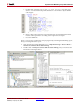
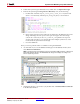
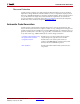
11. After the simulation is finished, you should be able to observe the simulation
waveforms as shown in the figure below:
All DCM clocks are included in the top-level wrapper testbench file
(hybrid_dcm_ce_case1_dcm_mcw_tb.vhd) – clk_1, clk_2 and clk_4.
Summary
When you select the Hybrid DCM-CE option, System Generator automatically infers and
instantiates a DCM without further manual intervention. In addition, the tool intelligently
generates different clock rates by using a combination of DCM and CE clock generation
algorithms and by assigning appropriate clock rates to either the DCM or CE in order to
obtain optimal Quality of Results and low power consumption. You do not have to set
attributes or specify DCM clock outputs. You should expect minimal clock skew when
selecting the Hybrid DCM-CE option compared to the Clock Enables option alone.
Tutorial Example: Using the Expose Clock Ports Option
The following step-by-step example will show you how to select the Expose Clock Ports
option, netlist the HDL design, implement the design in ISE, simulate the design, then
examine the files and reports to verify the design.
The expose_clock_ports_case1 design example is located at the following pathname
<ISE_Design_Suite_tree>/sysgen>/examples/clocking_options/expose_c
lock_ports_case1/expose_clock_ports_case1.mdl
1. Open the model in MATLAB and observe the following blocks:
• Addressable Shift Register (ASR): used to implement the input delay buffer. The
address port runs n times faster than the data port, where n is the number of the filter
taps (5 for this example)
• Coefficient ROM: used to store the filter coefficients
• Counter: used to generate addresses for the ROM and ASR
• Comparator: used to generate the reset and enable signals