
User guide

System Generator for DSP User Guide www.xilinx.com 267
UG640 (v 12.2) July 23, 2010
Real-Time Signal Processing using Hardware Co-Simulation
Real-Time Signal Processing using Hardware Co-Simulation
The shared memory interfaces available in System Generator allow signal processing
designs with high bandwidth and memory requirements to be co-simulated using FPGA
hardware. When used in conjunction with the Xilinx Shared Memory Read and Write
blocks, it is possible for hardware co-simulation designs to process complete Simulink
vector and matrix signals in a single simulation cycle. These large data transactions
between Simulink and the FPGA are realized using burst transfers, and depending on the
co-simulation interface, often provide sufficient throughput for real-time signal processing
applications.
There are two types of System Generator interfaces that support burst transfers when
compiled into FPGA hardware. These interfaces include lockable shared memories and
shared FIFO blocks. Both blocks provide different handshaking protocols that determine
how and when transactions between the FPGA and host PC occur. Before using these
blocks, it is useful to understand how they work in relation to hardware co-simulation. For
more information, please refer to the following topics:
Co-Simulating Lockable Shared Memories
Co-Simulating Shared FIFOs
In this document, a high-speed co-simulation buffering interface implemented as a System
Generator model is presented. The example interface uses lockable-shared memories to
implement the required buffer storage. Note that it is relatively straightforward to modify
the flow control logic so that shared FIFOs may be used in place of the shared memories.
The high-speed buffering interface is discussed first, followed by an example in which the
interface is used to support real-time processing of a video stream using a 5x5 filter kernel.
Described last is how an additional unprotected shared memory is applied to the system to
support dynamic reloading of the image kernel during co-simulation.
Shared Memory I/O Buffering Example
When a lockable shared memory is compiled for hardware co-simulation, additional
circuitry is included in the FPGA to the handle the mutual exclusion. Part of this circuitry
includes logic to enable high-speed transfers of the memory image when the FPGA
acquires or releases lock of the memory. It takes advantage of the lockable shared memory
mutual exclusion semantics to implement a high-speed I/O buffering interface for
hardware co-simulation. This topic describes this interface, which is included as an
example model in your System Generator software installation.
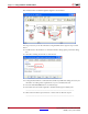
1. From the MATLAB console, change directory to
<ISE_Design_Suite_tree>/sysgen/examples/shared_memory/hardware_
cosim/io_bufferin
2. Open highspeed_iobuf_ex.mdl from the MATLAB console.
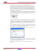
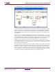
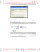
The I/O buffering interface allows you to easily buffer and stream data through a System
Generator signal processing data path during hardware co-simulation. The example
design is comprised of two subsystems that implement input and output buffer storage,
named Input Buffer and Output Buffer, respectively. The turquoise block in the center of
the diagram is a placeholder for the signal processing data path which you will substitute
into the design.
At the heart of each buffering subsystem is a lockable shared memory block that provides
the buffer storage. Each shared memory is wrapped by logic that controls the flow of data