
User guide

System Generator for DSP User Guide www.xilinx.com 265
UG640 (v 12.2) July 23, 2010
Frame-Based Acceleration using Hardware Co-Simulation
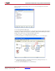
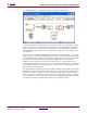
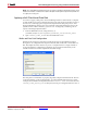
21. Add the hardware co-simulation block to the design as shown below.
As mentioned before, the Shared Memory Write block writes a new input frame of 4095
words to the FPGA on every 4095th clock cycle. Likewise, the Shared Memory Read block
reads an output frame of 4095 words from the FPGA on every 4095th clock cycle. This
means that the FPGA must process the entire frame in a single-cycle. How exactly is this
accomplished?
The first step is to configure the FPGA in free-running clock mode. In doing so, you allow
the FPGA to process data considerably faster than if it were otherwise kept in lockstep with
the Simulink simulation. Whereas in single-step mode the FPGA can only process one data
per Simulink cycle, the FPGA processing speed is limited only by the system clock
frequency when operating in free-running clock mode. Even so, if the buffer is large
enough, the FPGA may not have time to process the complete buffer before the next block
in the design is woken up. You still need a way to stall the rest of the simulation while the
FPGA processes the entire buffer.
The Shared Memory Read block checks the number of FIFO words available in the output
buffer before trying to read a frame. If the number of words in the buffer is insufficient, the
Read block waits for a small amount of time, and then checks again to determine if the
words have become available. It only reads the frame once all of the words are available in
the output buffer, in this case 4095. In this manner, the Shared Memory Read block can stall
the simulation until the complete frame has been processed by the FPGA.