
User guide

250 www.xilinx.com System Generator for DSP User Guide
UG640 (v 12.2) July 23, 2010
Chapter 3: Using Hardware Co-Simulation
Asynchronous FIFOs are typically used in multi-clock applications to safely cross clock
domain boundaries. When a Free-Running Clock mode is used for hardware co-
simulation, the FPGA operates asynchronously relative to the Simulink simulation. That is,
the FPGA is not kept in lockstep with the simulation. Using the Free-Running Clock mode
effectively establishes two clock domains: the Simulink simulation clock domain and the
FPGA free-running clock domain. In these designs, Shared FIFOs provide a reliable and
safe way to transfer data between the host PC and FPGA board.
Shared FIFOs may also be used to support burst transfers during co-simulation. It is
possible to create vectors or frames of data, and transfer the data to the FPGA in a single
transaction with the hardware. These interfaces can be used to further accelerate
simulation speeds beyond what is typically possible with hardware co-simulation. For
more information on how this is accomplished, refer to the topic Frame-Based Acceleration
using Hardware Co-Simulation.
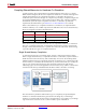
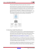
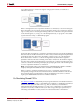
When a shared FIFO pair is generated for co-simulation, a single asynchronous FIFO core
replaces the two software shared FIFO blocks. As shown in the figure below, the read /
write FIFO sides are attached to user design logic (i.e., logic derived from the original
System Generator model) that attached to the From FIFO and To FIFO blocks. Because both
FIFO sides attach to user logic in hardware, the PC does not share control of the FIFO with
the design. Instead, the FIFO behavior is similar to a System Generator design that
includes a traditional FIFO block.
Note that even though the FIFO exposes independent clock ports, the same co-simulation
clock drives both ports when a FIFO pair is compiled. This is different from compiling a
shared FIFO pair using the Multiple Subsystem Generator
block, where the clocks are from
distinct clock domains.
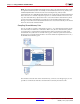
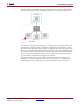
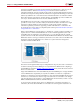
Single shared FIFO blocks are treated differently than shared FIFO pairs. A single To FIFO
or From FIFO block is replaced by an asynchronous FIFO core when it is compiled for
hardware co-simulation. One side of the FIFO (i.e., the unused shared FIFO half in System
Generator) is connected to PC interface logic. The other side is connected to user design
logic that attached to the original To or From FIFO block. In this manner, control over the
FIFO is distributed between the PC and FPGA design.
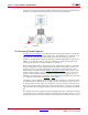
As shown in the following figure, when a To FIFO block is compiled for hardware co-
simulation, the write side of the FIFO is connected to the same logic that attached to To