
User guide

System Generator for DSP User Guide www.xilinx.com 159
UG640 (v 12.2) July 23, 2010
Integrating a Processor with Custom Logic
When a System Generator model contains an XPS project imported through the EDK
Processor block in single clock mode, the XPS project is driven by the clock generated by
the Hardware Co-Simulation module. This allows the processor to be simulated in lock-
step with the rest of the DUT and the Simulink simulation. This kind of simulation can be
very helpful when you are debugging transactions over a custom bus or when you are
profiling code.
Limitations with the XPS Clock Generator
An XPS project created using BSB (Base System Builder) usually includes a clock generator,
which is used to generate clock signals with requested frequencies to drive the MicroBlaze
processor and other peripherals such as DDR3 external memory and Ethernet MAC.
Similar to the hardware co-simulation module, the clock generator generates the requested
clock frequencies using DCM/MMCM/PLL.
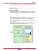
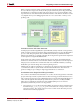
In the single-clock wiring scheme depicted in the previous figure, the DCM inside the
hardware co-simulation clock control module and the clock generator from the imported
XPS project are cascaded. For some FPGA boards such as ML506 and SP601, cascading
DCM/PLLs prevents the design from achieving timing closure.
Additionally, in single-step hardware co-simulation, the output clock from the hardware
co-simulation module is synchronized with the Simulink simulation. The XPS clock
generator simply stops working in single-stepped hardware co-simulation.
One Solution to the Single-Clock Wiring Limitations
One solution to the limitation described above is to take out the clock generator in the XPS
project and re-import it into System Generator. The following procedure illustrates how to
take out the clock generator using a ML506-based project generated using BSB. While you
can do this through the XPS GUI, this procedure shows you how to modify the MHS
(Microprocessor Hardware Specification) file and MSS (Microprocessor Software
Specification) file directly to remove clock generator.
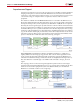
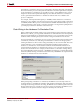
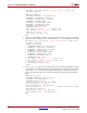
1. The original
system.mhs file created using BSB is shown below. Observe that the input
board clock
fpga_0_clk_1_sys_clk_pin is connected to the CLKIN pin of the clock
generator instance. The output clock pin
CLKOUT0 is then used to drive the processor
and the other hardware peripherals.