
User guide

System Generator for DSP User Guide www.xilinx.com 157
UG640 (v 12.2) July 23, 2010
Integrating a Processor with Custom Logic
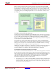
The third advantage is that designs compiled with the dual-clock wiring scheme tend to
meet timing more easily compared with the single-clock wiring scheme. With the dual-
clock wiring scheme, the DCM in the hardware co-simulation clock control module and
the clock generator in the imported XPS project are not cascaded (as is the case when
single-clock wiring is used). This greatly improves the chances of meeting timing when
generating the Hardware Co-Simulation block with the imported XPS project.
Limitations for Boards with Multiple-Input Clocks
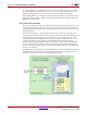
In the dual-clock wiring scheme, both the hardware co-simulation clock control module
and the imported XPS project are driven by the board input clock specified by the
hardware co-simulation compilation target. For FPGA boards with multiple clock sources,
it is possible that the imported XPS project uses a different board input clock than the
System Generator hardware co-simulation compilation target.
An example is the ML506 FPGA board. The ML506 FPGA board has two input clock
sources, one crystal 100 MHz input clock and one LVDS 200 MHz input clock. The XPS
project generated by Base System Builder uses the 100 MHz input clock, while the System
Generator ML506 hardware co-simulation compilation target uses the LVDS 200 MHz
input clock.
The following procedure uses the ML506 board to illustrate how to change the clock
sources in an XPS project in order to match the input clock source used by System
Generator hardware co-simulation.
1. Find out the frequency of the board input clock used by the System Generator
hardware co-simulation target. For the JTAG ML506 hardware co-simulation
compilation target, you can look at the file
<sysgen>/plugins/compilation/Hardware Co-Simulation/ML506/JTAG/
ML506_JTAG.ucf
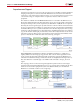
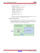
2. Verify that the board input clock frequency is 200 MHz. Another way to find out the
board input clock source is to run the hardware co-simulation compilation target once
and look at the file
<netlist_dir>/jtagcosim_top.ucf. In the following snippet of
the file
ML506_JTAG.ucf, you can see that the System Generator hardware co-
simulation uses a 200 MHz LVDS board input clock source.
NET "sys_clk_p" LOC = "L19";
NET "sys_clk_n" LOC = "K19";
NET "sys_clk_p" TNM_NET = "hwcosim_sys_clk";
NET "sys_clk_n" TNM_NET = "hwcosim_sys_clk";
TIMESPEC "TS_hwcosim_sys_clk" = PERIOD "hwcosim_sys_clk" 200 MHz HIGH
50%;
3. In the system.mhs file found in the XPS project, change the input clock frequency from
100 MHz to 200 MHz, which is the frequency of the clock source used by the System
Generator hardware co-simulation compilation target.
PORT fpga_0_clk_1_sys_clk_pin = dcm_clk_s, DIR = I, SIGIS = CLK,
CLK_FREQ = 200000000