
User guide

134 www.xilinx.com System Generator for DSP User Guide
UG640 (v 12.2) July 23, 2010
Chapter 1: Hardware Design Using System Generator
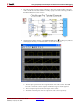
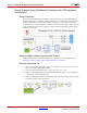
7. Connecting the ChipScope Block
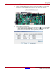
The signal used to trigger ChipScope is the counter output. The two buses that you
want to probe are the sine and cosine from the Sine/Cosine table. Connect the signals
appropriately as shown on the following figure:
Note that the names of the ports on the ChipScope block are specified by names given
to the signals connected to the block, e.g. Sine and Cosine.
8. Location Constraints
Now that the design is fully implemented and simulates correctly, the next step is to
prepare it for connection to the hardware target. Although it can work on any
hardware platform, the process is described for the ML506.
Two pins need to be locked down in this design: The LED and the clock pin.
♦ LED Pin: Double click on the Gateway Out1 block, select Specify IOB Location
constraints and type in {'AE24'} (note the need for single quotes).
♦ Clock Pin: Double click on the System Generator block, set the clock period to
10ns and the clock pin location to AH15.
If you are using a different board, the pin locations should be modified appropriately.
9. System Generator GUI settings
The last two parameters that should be updated before generating a bitstream are the
target device and the compilation target.