
User guide

124 www.xilinx.com System Generator for DSP User Guide
UG640 (v 12.2) July 23, 2010
Chapter 1: Hardware Design Using System Generator
subsystems to determine their output, hence different system periods yield different
system clocks.
Now consider the clocks defined by the System Generator block in the ss_clk_domainA
and ss_clk_domainB subsystems.
5. Open the System Generator block parameter dialog boxes inside the
ss_clk_domainA and ss_clk_domainB subsystems.
The System Generator block dialog box in the ss_clk_domainA subsystem defines an
FPGA clock period of 10ns (i.e., a frequency of 100MHz). To simplify the sample period
values in the model, the 10 ns clock is normalized to a Simulink system period value of 2
sec. In the ss_clk_domainB subsystem, an FPGA clock period of 15ns (i.e., a frequency
66.7 MHz) is defined. Normalizing this clock period gives us a Simulink system period
value of 3 sec.
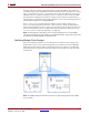
Because the two subsystems in this example implement multiple, synchronous, System
Generator domains, you will use the Multiple Subsystem Generator block to wire the
subsystems together into a single HDL top-level component that exposes two clock ports.
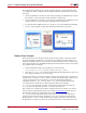
When the Multiple Subsystem Generator translates a design into hardware, it generates
each subsystem individually as an NGC netlist file. It also creates a top-level VHDL
component or Verilog module that instantiates the subsystem netlist files as black boxes,
and wires them together using shared memory cores as clock domain bridges.
You begin by using the Multiple Subsystem Generator block to netlist subsystems
ss_clk_domainA and ss_clk_domainB.
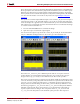
6. Open the Multiple Subsystem Generator dialog box by double clicking on the Multiple
Subsystem Generator block included in the top-level of the two_async_clks model.
7. Pick a suitable target directory inside the Multiple Subsystem Generator dialog box.
The default directory is netlist.