
User guide

System Generator for DSP User Guide www.xilinx.com 121
UG640 (v 12.2) July 23, 2010
Generating Multiple Cycle-True Islands for Distinct Clocks
member of the pair resides in a different domain. Because the RAM is a true dual-port,
each domain may write to the RAM. Care must be taken, by means of semaphores or other
logic, to ensure that two writes or a read and a write to the same address do not happen
simultaneously. For example, if domain A writes to a memory location at the same time
that domain B is reading from it, the data read may not be valid. The shared memory is
implemented as a using Xilinx Dual Port Block Memory core to ensure that large memories
are efficiently mapped across multiple BRAMs.
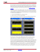
The To Register is put in the domain in which it is to be written, and the From
Register in the domain from which it is to be read. The two blocks are linked by the
name of the shared memory. The To Register may also be read synchronously in its own
domain. The register may be of variable width and will synthesize as flip-flops. A 1-bit
To/From Register pair will synthesize as a single flop.
Note:
Crossing domains in this manner can be unsafe, and requires the use of metastability-
reducing synchronization flops and semaphores for multiple-bit transfers. This technique should only
be used when the hardware pitfalls are well-understood.
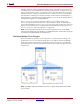
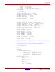
Netlisting Multiple Clock Designs
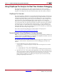
Each clock domain should have its own subsystem in a System Generator design. The
diagram below shows a two-domain design. The top-level block contains the Multiple
Subsystem Generator block and two subsystems which each comprise a clock domain.
Each subsystem has a System Generator block that sets the system clock period for that
clock domain.
Note:
The Multiple Subsystem Generator block does not support designs that include an EDK
Processor block