System Generator for DSP User Guide UG640 (v 12.
Xilinx is disclosing this user guide, manual, release note, and/or specification (the "Documentation") to you solely for use in the development of designs to operate with Xilinx hardware devices. You may not reproduce, distribute, republish, download, display, post, or transmit the Documentation in any form or by any means including, but not limited to, electronic, mechanical, photocopying, recording, or otherwise, without the prior written consent of Xilinx.
Table of Contents Preface: About This Guide Guide Contents . . . . . . . . . . . . . . . . . . . . . . . . . . . . . . . . . . . . . . . . . . . . . . . . . . . . . . . . . . . . . . 9 System Generator PDF Doc Set . . . . . . . . . . . . . . . . . . . . . . . . . . . . . . . . . . . . . . . . . . . . . . . 9 Additional Resources . . . . . . . . . . . . . . . . . . . . . . . . . . . . . . . . . . . . . . . . . . . . . . . . . . . . . . . . 9 Conventions . . . . . . . . . . . . . . . . . . . . . . . . . . . .
A Step-by-Step Example . . . . . . . . . . . . . . . . . . . . . . . . . . . . . . . . . . . . . . . . . . . . . . . . . . . 75 Configurable Subsystems and System Generator . . . . . . . . . . . . . . . . . . . . . . . . . . . . 83 Defining a Configurable Subsystem . . . . . . . . . . . . . . . . . . . . . . . . . . . . . . . . . . . . . . . . . Using a Configurable Subsystem . . . . . . . . . . . . . . . . . . . . . . . . . . . . . . . . . . . . . . . . . . .
EDK Processor Block . . . . . . . . . . . . . . . . . . . . . . . . . . . . . . . . . . . . . . . . . . . . . . . . . . . . . 144 Integrating a Processor with Custom Logic. . . . . . . . . . . . . . . . . . . . . . . . . . . . . . . . . . 144 Memory Map Creation . . . . . . . . . . . . . . . . . . . . . . . . . . . . . . . . . . . . . . . . . . . . . . . . . . . Hardware Generation . . . . . . . . . . . . . . . . . . . . . . . . . . . . . . . . . . . . . . . . . . . . . . . . . . . .
Restrictions on Shared Memories . . . . . . . . . . . . . . . . . . . . . . . . . . . . . . . . . . . . . . . . . . 252 Specifying Xilinx Tool Flow Settings . . . . . . . . . . . . . . . . . . . . . . . . . . . . . . . . . . . . . . . 252 Frame-Based Acceleration using Hardware Co-Simulation . . . . . . . . . . . . . . . . . . 254 Shared Memories . . . . . . . . . . . . . . . . . . . . . . . . . . . . . . . . . . . . . . . . . . . . . . . . . . . . . . . . Adding Buffers to a Design . . . . . . . . . . . .
Chapter 5: System Generator Compilation Types HDL Netlist Compilation . . . . . . . . . . . . . . . . . . . . . . . . . . . . . . . . . . . . . . . . . . . . . . . . . . 378 NGC Netlist Compilation . . . . . . . . . . . . . . . . . . . . . . . . . . . . . . . . . . . . . . . . . . . . . . . . . . 378 Bitstream Compilation . . . . . . . . . . . . . . . . . . . . . . . . . . . . . . . . . . . . . . . . . . . . . . . . . . . . . 379 XFLOW Option Files . . . . . . . . . . . . . . . . . . . . . . . . . . . . . .
www.xilinx.com System Generator for DSP User Guide UG640 (v 12.
Preface About This Guide This User Guide provides in-depth discussions on topics that are key to understanding and using System Generator. In addition, examples and turorials are also provided that extend beyond the scope of the System Generator Getting Started Guide.
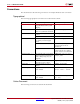
Preface: About This Guide Conventions This document uses the following conventions. An example illustrates each convention.
Conventions Convention Blue text Meaning or Use Example Cross-reference link to a location in the current document See the topic “Additional Resources” for details. Red text Cross-reference link to a location in another document See Figure 2-5 in the Virtex-II Platform FPGA User Guide. Blue, underlined text Hyperlink to a website (URL) Go to http://www.xilinx.com for the latest speed files. System Generator for DSP User Guide UG640 (v 12.2) July 23, 2010 www.xilinx.
Preface: About This Guide 12 www.xilinx.com System Generator for DSP User Guide UG640 (v 12.
Chapter 1 Hardware Design Using System Generator System Generator is a system-level modeling tool that facilitates FPGA hardware design. It extends Simulink in many ways to provide a modeling environment that is well suited to hardware design. The tool provides high-level abstractions that are automatically compiled into an FPGA at the push of a button. The tool also provides access to underlying FPGA resources through low-level abstractions, allowing the construction of highly efficient FPGA designs.
Chapter 1: Hardware Design Using System Generator Notes for Higher Performance FPGA Design Suggests design practices in System Generator that lead to an efficient and high-performance implementation in an FPGA. Processing a System Generator Design with FPGA Physical Design Tools Describes how to take the low-level HDL produced by System Generator and use it in tools like Xilinx's Project Navigator, ModelSim, and Synplicity's Synplify.
A Brief Introduction to FPGAs MHz are common today) and a highly-distributed memory architecture gives the system designer an ability to exploit parallelism in DSP (and other) applications that operate on data streams. For example, the raw memory bandwidth of a large FPGA running at a clock rate of 150 MHz can be hundreds of terabytes per second. There are many DSP applications (e.g.
Chapter 1: Hardware Design Using System Generator logic abstractions to build very high performance digital filters, FFTs, and other arithmetic and signal processing functions. While the multiply-accumulate function supported by a Virtex®-4 DSP block is familiar to a DSP engineer, it is instructive to take a closer look at the Virtex® FPGA family logic slice (shown below), which is the fundamental unit of the logic fabric array.
A Brief Introduction to FPGAs division multiplexed (TDM) data streams. The addressable shift register (ASR) block, with a function depicted in the figure below, provides an arbitrary width, arbitrary depth tapped delay line. This block is of particular interest to the DSP engineer, since it can be used to implement tapped delay lines as well as sweeping through TDM data streams.
Chapter 1: Hardware Design Using System Generator have detailed knowledge of the underlying FPGA details. However, when it makes sense to implement an algorithm using basic functions (e.g., adder, register, memory), System Generator allows you to exploit your FPGA knowledge while reducing the clerical tasks of managing all signals explicitly. System Generator library blocks and the mapping from Simulink to hardware are described in detail in subsequent topics of this documentation.
Design Flows using System Generator Algorithm Exploration System Generator is particularly useful for algorithm exploration, design prototyping, and model analysis. When these are the goals, you can use the tool to flesh out an algorithm in order to get a feel for the design problems that are likely to be faced, and perhaps to estimate the cost and performance of an implementation in hardware. The work is preparatory, and there is little need to translate the design into hardware.
Chapter 1: Hardware Design Using System Generator System-Level Modeling in System Generator System Generator allows device-specific hardware designs to be constructed directly in a flexible high-level system modeling environment. In a System Generator design, signals are not just bits. They can be signed and unsigned fixed-point numbers, and changes to the design automatically translate into appropriate changes in signal types. Blocks are not just stand-ins for hardware.
System-Level Modeling in System Generator System Generator Blocksets A Simulink blockset is a library of blocks that can be connected in the Simulink block editor to create functional models of a dynamical system. For system modeling, System Generator blocksets are used like other Simulink blocksets. The blocks provide abstractions of mathematical, logic, memory, and DSP functions that can be used to build sophisticated signal processing (and other) systems.
Chapter 1: Hardware Design Using System Generator Xilinx Blockset The Xilinx Blockset is a family of libraries that contain basic System Generator blocks. Some blocks are low-level, providing access to device-specific hardware. Others are highlevel, implementing (for example) signal processing and advanced communications algorithms. For convenience, blocks with broad applicability (e.g., the Gateway I/O blocks) are members of several libraries. Every block is contained in the Index library.
System-Level Modeling in System Generator description of its implementation and hardware resource requirements. Individual documentation for each block is also provided in the topic Xilinx Reference Blockset. Signal Types In order to provide bit-accurate simulation of hardware, System Generator blocks operate on Boolean and arbitrary precision fixed-point values. By contrast, the fundamental scalar signal type in Simulink is double precision floating point.
Chapter 1: Hardware Design Using System Generator In the System Generator portion of a Simulink model, every signal must be sampled. Sample times may be inherited using Simulink's propagation rules, or set explicitly in a block customization dialog box. When there are feedback loops, System Generator is sometimes unable to deduce sample periods and/or signal types, in which case the tool issues an error message. Assert blocks must be inserted into loops to address this problem.
System-Level Modeling in System Generator Simulink scope), but does not alter sample rates. The scope output below shows the unaltered and sampled versions of the sine wave. Multirate Models System Generator supports multirate designs, i.e., designs having signals running at several sample rates. System Generator automatically compiles multirate models into hardware. This allows multirate designs to be implemented in a way that is both natural and straightforward in Simulink.
Chapter 1: Hardware Design Using System Generator Hardware Oversampling Some System Generator blocks are oversampled, i.e., their internal processing is done at a rate that is faster than their data rates. In hardware, this means that the block requires more than one clock cycle to process a data sample. In Simulink such blocks do not have an observable effect on sample rates. One block that can be oversampled is the DAFIR FIR filter.
System-Level Modeling in System Generator The Clock Enables Option When System Generator compiles a model into hardware with the Clock Enable option selected, System Generator preserves the sample rate information of the design in such a way that corresponding portions in hardware run at appropriate rates. In hardware, System Generator generates related rates by using a single clock in conjunction with clock enables, one enable per rate.
Chapter 1: Hardware Design Using System Generator A dcm_reset input port is exposed on the top-level wrapper to allow the external design to reset the DCM after bitstream configuration. A dcm_locked output port is also exposed to help the external design synchronize the input data with the single clk input port.
System-Level Modeling in System Generator • Addressable Shift Register (ASR): used to implement the input delay buffer.
Chapter 1: Hardware Design Using System Generator 2. Double-click on the System Generator token to bring up the following dialog box: As shown, select Hybrid DCM-CE, then click Generate. After a few moments, a subdirectory named hdl_netlist_dcm is created in the current working directory containing the generated files. 30 3. In the MATLAB Current Directory window, double-click on the file hybrid_dcm_ce_case1_sysgen.log.
System-Level Modeling in System Generator a. Double-click on the file hybrid_dcm_ce_case1_dcm_mcw.vhd, then scroll down to view the DCM component declaration as shown below by the VHDL code snippet: b. Observe that System Generator automatically infers and instantiates the DCM instance and its parameters according to the required clock outputs. c. Close the VHDL file. Next, you are going to examine the clock propagation by examining the ISE timing report. First, you must generate the report. 7.
Chapter 1: Hardware Design Using System Generator This design is comprised of six clock rates – 1, 2, 4, 8, 20, 40 with respect to the 10 ns global clock constraint.
System-Level Modeling in System Generator 11. After the simulation is finished, you should be able to observe the simulation waveforms as shown in the figure below: All DCM clocks are included in the top-level wrapper testbench file (hybrid_dcm_ce_case1_dcm_mcw_tb.vhd) – clk_1, clk_2 and clk_4. Summary When you select the Hybrid DCM-CE option, System Generator automatically infers and instantiates a DCM without further manual intervention.
Chapter 1: Hardware Design Using System Generator • MAC Engine: used as a Multiply-Accumulator operator for the filter 2. Double-click on the System Generator token to bring up the following dialog box: As shown above, select Expose Clock Ports, then click Generate. After a few moments, a sub-directory named hdl_netlist is created in the current working directory containing the generated files. 3. 34 Launch ISE, then load the ISE project at pathname ./hdl_netlist/expose_clock_ports_case1_mcw.
System-Level Modeling in System Generator 4. Under the Project Navigator Processes view, double-click on Implement Design. 5. From the Project Navigator Design Sources Hierarchy view, do the following: a. Double-click on the file expose_clock_ports_case1_mcw.vhd, then scroll down to view the entity named expose_clock_ports_mcw, as shown below: b. Observe that System Generator infers the clocks based on the different rates in the design and brings the clock ports to the top-level wrapper.
Chapter 1: Hardware Design Using System Generator 8. After the simulation is finished, you should be able to observe the simulation waveforms as shown in the figure below: Summary When you select the Expose Clock Ports option, System Generator automatically infers the correct clocks from the design rates and exposes the clock ports in the top-level wrapper. The clock rates are determined by the same methodology when you use the Clock Enables option.
System-Level Modeling in System Generator NaNs that drive a Gateway In become indeterminate values. System Generator provides an Indeterminate Probe block that allows for the detection of indeterminate values. This probe cannot be translated into hardware. In System Generator, any arithmetic signal can be indeterminate, but Boolean signals cannot be. If a simulation reaches a condition that would force a Boolean to become indeterminate, the simulation is halted and an error is reported.
Chapter 1: Hardware Design Using System Generator As shown below, in the parameter editing dialog for the accumulator and multiplier blocks, there are radio buttons that allow either the truncate or round option to be selected. In order to use a parameter rather than the radio button selection, right click on the radio button and select: “Define With Expression”. A MATLAB expression can then be used as the parameter setting.
Automatic Code Generation Resource Estimation System Generator supplies tools that estimate the FPGA hardware resources needed to implement a design. Estimates include numbers of slices, lookup tables, flip-flops, block memories, embedded multipliers, I/O blocks and tristate buffers. These estimates make it easy to determine how design choices affect hardware requirements.
Chapter 1: Hardware Design Using System Generator Compiling and Simulating Using the System Generator Block System Generator automatically compiles designs into low-level representations. Designs are compiled and simulated using the System Generator block. This topic describes how to use the block. Before a System Generator design can be simulated or translated into hardware, the design must include a System Generator block.
Automatic Code Generation Compilation Type and the Generate Button Pressing the Generate button instructs System Generator to compile a portion of the design into equivalent low-level results. The portion that is compiled is the sub-tree whose root is the subsystem containing the block. (To compile the entire design, use a System Generator block placed at the top of the design.) The compilation type (under Compilation) specifies the type of result that should be produced.
Chapter 1: Hardware Design Using System Generator Control Description Synthesis tool Specifies the tool to be used to synthesize the design. The possibilities are Synplify, Synplify Pro and Xilinx XST. Hardware description language Specifies the language to be used for HDL netlist of the design. The possibilities are VHDL and Verilog. Create testbench This instructs System Generator to create an HDL testbench.
Automatic Code Generation Control Description DCM input clock period(ns) Specify if different than the FPGA clock period(ns) option (system clock). The FPGA clock period (system clock) will then be derived from this hardware-defined input. Provide clock enable clear pin This instructs System Generator to provide a ce_clr port on the toplevel clock wrapper. The ce_clr signal is used to reset the clock enable generation logic.
Chapter 1: Hardware Design Using System Generator Hierarchical Controls The Simulink System Period control (see the topic Simulink System Period above) on the System Generator block is hierarchical. A hierarchical control on a System Generator block applies to the portion of the design within the scope of the block, but can be overridden on other System Generator blocks deeper in the design.
Automatic Code Generation no testbench is requested, then the key files produced by System Generator are the following: File Name or Type Description .vhd/.v This contains most of the HDL for the design _cw.vhd/.v This is a HDL wrapper for _files.vhd/.v. It drives clocks and clock enables. .edn and .ngc files Besides writing HDL, System Generator runs CORE Generator™ (coregen) to implement portions of the design.
Chapter 1: Hardware Design Using System Generator Using the System Generator Constraints File When a design is compiled, System Generator produces a constraints file that tells downstream tools how to process the design. This enables the tools to produce a higher quality implementation, and to do so using considerably less time.
Automatic Code Generation Constraints Example The figure below shows a small multirate design and the constraints System Generator produces for it. The up sampler doubles the rate, and the down sampler divides the rate by three. Assume the system clock period is 10 ns. Then the clock periods are 10 ns for the FIR, 20 ns for the input register, and 30 ns for the output register. The following text describes the constraints that convey this information.
Chapter 1: Hardware Design Using System Generator Group to group constraints establish relative speeds. Here are the constraints that relate the speeds of ce_2_392b7670_group and ce_3_392b7670_group: # Group-to-group constraints TIMESPEC "TS_ce_2_392b7670_group_to_ce_3_392b7670_group" = FROM "ce_2_392b7670_group" TO "ce_3_392b7670_group" 20.0 ns; TIMESPEC "TS_ce_3_392b7670_group_to_ce_2_392b7670_group" = FROM "ce_3_392b7670_group" TO "ce_2_392b7670_group" 20.
Automatic Code Generation added to a larger design, but the clock wrapper is omitted. In this case, you are responsible for generating clocks and clock enables, but a finer degree of control is obtained. If, on the other hand, the clock wrapper is suitable for the application, then include it. The names of the clocks and clock enables in System Generator HDL suggest that clocking is completely general, but this is not the case.
Chapter 1: Hardware Design Using System Generator The “Expose Clock Ports” Multirate Implementation When you select this option, System Generator creates a top-level wrapper that exposes a clock port for each rate. You can then manually instantiate a clock generator outside the design to drive the clock ports. For a detailed examination of the files produced by this option, refer to the topic Tutorial Example: Using the Expose Clock Ports Option.
Compiling MATLAB into an FPGA Compiling MATLAB into an FPGA System Generator provides direct support for MATLAB through the MCode block. The MCode block applies input values to an M-function for evaluation using Xilinx's fixedpoint data type. The evaluation is done once for each sample period. The block is capable of keeping internal states with the use of persistent state variables.
Chapter 1: Hardware Design Using System Generator else z = y; end The xlmax.m file should be either saved in the same directory of the model file or should be in the MATLAB path. Once the xlmax.m has been saved to the appropriate place, you should drag a MCode block into your model, open the block parameter dialog box, and enter xlmax into the MATLAB Function field. After clicking the OK button, the block has two input ports x and y, and one output port z.
Compiling MATLAB into an FPGA % supported by the Xilinx MCode block. The function uses xfix() % to create Xilinx fixed-point numbers with appropriate % container types.% % You must use a xfix() to specify type, number of bits, and % binary point position to convert floating point values to % Xilinx fixed-point constants or variables. % By default, the xfix call uses xlTruncate % and xlWrap for quantization and overflow modes. % const1 is Ufix_8_3 const1 = xfix({xlUnsigned, 8, 3}, 1.
Chapter 1: Hardware Design Using System Generator After setting the dialog box parameter MATLAB Function to xlSimpleArith, the block shows two input ports a and b, and four output ports z1, z2, z3, and z4. 54 www.xilinx.com System Generator for DSP User Guide UG640 (v 12.
Compiling MATLAB into an FPGA M-functions using Xilinx data types and functions can be tested in the MATLAB command window. For example, if you type: [z1, z2, z3, z4] = xlSimpleArith(2, 3) in the MATLAB command window, you'll get the following lines: UFix(9, 3): 3.500000 Fix(12, 4): -8.687500 Fix(12, 8): 7.996094 Bool: true Notice that the two integer arguments (2 and 3) are converted to fixed-point numbers automatically. If you have a floating-point number as an argument, an xfix call is required.
Chapter 1: Hardware Design Using System Generator Shift Operations This example shows how to implement bit-shift operations using the MCode block. Shift operations are accomplished with multiplication and division by powers of two. For example, multiplying by 4 is equivalent to a 2-bit left-shift, and dividing by 8 is equivalent to a 3-bit right-shift. Shift operations are implemented by moving the binary point position and if necessary, expanding the bit width.
Compiling MATLAB into an FPGA Passing Parameters into the MCode Block This example shows how to pass parameters into the MCode block. An input argument to an M-function can be interpreted either as an input port on the MCode block, or as a parameter internal to the block. The following M-code defines an M-function xl_sconvert is contained in file xl_sconvert.
Chapter 1: Hardware Design Using System Generator To pass parameters to each MCode block in the diagram above, you can click the Edit Interface button on the block GUI then set the values for the M-function arguments. The mask for MCode block signed convert 1 is shown below: 58 www.xilinx.com System Generator for DSP User Guide UG640 (v 12.
Compiling MATLAB into an FPGA The above interface window sets the M-function argument nbits to be 10 and binpt to be 5. The mask for the MCode block signed convert 2 is shown below: The above interface window sets the M-function argument nbits to be 8 and binpt to be 4. System Generator for DSP User Guide UG640 (v 12.2) July 23, 2010 www.xilinx.
Chapter 1: Hardware Design Using System Generator Optional Input Ports This example shows how to use the parameter passing mechanism of MCode blocks to specify whether or not to use optional input ports on MCode blocks. The following M-code, which defines M-function xl_m_addsub is contained in file xl_m_addsub.m: function s = xl_m_addsub(a, b, sub) if sub s = a - b; else s = a + b; end The following diagram shows a subsystem containing two MCode blocks that use Mfunction xl_m_addsub. 60 www.xilinx.
Compiling MATLAB into an FPGA The Block Interface Editor of the MCode block labeled add is shown in below. As a result, the add block features two input ports a and b; it performs full precision addition. Input parameter sub of the MCode block labeled addsub is not bound with any value. Consequently, the addsub block features three input ports: a, b, and sub; it performs full precision addition or subtraction based on the value of input port sub. System Generator for DSP User Guide UG640 (v 12.
Chapter 1: Hardware Design Using System Generator Finite State Machines This example shows how to create a finite state machine using the MCode block with internal state variables. The state machine illustrated below detects the pattern 1011 in an input stream of bits. The M-function that is used by the MCode block contains a transition function, which computes the next state based on the current state and the current input.
Compiling MATLAB into an FPGA state = seen_10; end case seen_10 % seen 10 if din==1 state = seen_101; else % no part of sequence seen, go to seen_none state = seen_none; end case seen_101 if din==1 state = seen_1; matched = true; else state = seen_10; matched = false; end end The following diagram shows a state machine subsystem containing a MCode block after compilation; the MCode block uses M-function detect1101_w_state.
Chapter 1: Hardware Design Using System Generator end else if ~en else % if enabled, update the state if op==0 s = s/feed_back_down_scale + b; else s = s/feed_back_down_scale - b; end end end The following diagram shows a subsystem containing the accumulator MCode block using M-function xl_accum. The MCode block is labeled MCode Accumulator. The subsystem also contains the Xilinx Accumulator block, labeled Accumulator, for comparison purposes.
Compiling MATLAB into an FPGA Optional inputs rst and load of block Accum_MCode1 are disabled in the cell array of the Function Parameter Bindings parameter. The block mask for block MCode Accumulator is shown below: System Generator for DSP User Guide UG640 (v 12.2) July 23, 2010 www.xilinx.
Chapter 1: Hardware Design Using System Generator The example contains two additional accumulator subsystems with MCode blocks using the same M-function, but different parameter settings to accomplish different accumulator implementations. FIR Example and System Verification This example shows how to use the MCode block to model FIRs. It also shows how to do system verification with the MCode block. The model contains two FIR blocks. Both are modeled with the MCode block and both are synthesizable.
Compiling MATLAB into an FPGA error('latency must be at least 1'); end lat = lat - 1; persistent dly, if lat <= 0 y = reg_line.back; else dly = xl_state(zeros(1, lat), out_prec, lat); y = dly.back; dly.push_front_pop_back(reg_line.back); end for idx = len-1:-1:1 reg_line(idx) = reg_line(idx - 1) + coef_vec(len - idx - 1) * x; end reg_line(0) = coef_vec(len - 1) * x; The parameters are configured as following: System Generator for DSP User Guide UG640 (v 12.2) July 23, 2010 www.xilinx.
Chapter 1: Hardware Design Using System Generator In order to verify that the functionality of two blocks are equal, we also use another MCode block to compare the outputs of two blocks. If the two outputs are not equal at any given time, the error checking block will report the error.
Compiling MATLAB into an FPGA RPN Calculator This example shows how to use the MCode block to model a RPN calculator which is a stack machine. The block is synthesizable. The following function models the RPN calculator.
Chapter 1: Hardware Design Using System Generator OP_DROP = 6; q = acc; active = acc_active; if rst acc = 0; acc_active = false; stack_pt = 0; elseif en if ~is_oper % enter data, push if acc_active stack_pt = xfix(stack_pt_prec, stack_pt + 1); mem(stack_pt) = acc; stack_active = true; else acc_active = true; end acc = din; else if op == OP_NEG % unary op, no stack op acc = -acc; elseif stack_active b = mem(stack_pt); switch double(op) case OP_ADD acc = acc + b; case OP_SUB acc = b - acc ; case OP_MULT acc
Compiling MATLAB into an FPGA Example of disp Function The following MCode function shows how to use the disp function to print variable values. function x = testdisp(a, b) persistent dly, dly = xl_state(zeros(1, 8), a); persistent rom, rom = xl_state([3, 2, 1, 0], a); disp('Hello World!'); disp(['num2str(dly) is ', num2str(dly)]); disp('disp(dly) is '); disp(dly); disp('disp(rom) is '); disp(rom); a2 = dly.back; dly.push_front_pop_back(a); x = a + b; disp(['a = ', num2str(a), ', ', ...
Chapter 1: Hardware Design Using System Generator Here are the lines that are displayed on the MATLAB console for the first simulation step. mcode_block_disp/MCode (Simulink time: 0.000000, FPGA clock: 0) Hello World! num2str(dly) is [0.000000, 0.000000, 0.000000, 0.000000, 0.000000, 0.000000, 0.000000, 0.000000] disp(dly) is type: Fix_11_7, maxlen: 8, length: 8, 0: binary 0000.0000000, double 0.000000, 1: binary 0000.0000000, double 0.000000, 2: binary 0000.0000000, double 0.000000, 3: binary 0000.
Importing a System Generator Design into a Bigger System Importing a System Generator Design into a Bigger System A System Generator design is often a sub-design that is incorporated into a larger HDL design. This topic shows how to embed two System Generator designs into a larger design and how VHDL created by System Generator can be incorporated into the simulation model of the overall system. Starting with Release 10.
Chapter 1: Hardware Design Using System Generator New Integration Flow between System Generator & Project Navigator The illustration below shows the entire flow of how multiple System Generator designs can be integrated into Project Navigator as lower-level designs. System Generator generates a project file with an extension .sgp that you can add as a System Generator source type in Project Navigator.
Importing a System Generator Design into a Bigger System A Step-by-Step Example In this example, two HDL netlists from System Generator are integrated into a larger VHDL design. Design #1 is named SPRAM and design #2 is named MAC_FIR. The toplevel VHDL entity combines the two data ports and a control signal from the SPRAM design to create a bidirectional bus. The top-level VHDL also instantiates the MAC_FIR design and supplies a separate clock signal named clk2.
Chapter 1: Hardware Design Using System Generator Generating the HDL Files for the System Generator Designs The steps used to create the HDL files are as follows: 1. Open the first design, spram.mdl, in MATLAB. This is a multirate design due to the down sampling block placed after the output of the Single Port RAM. 2. Double click on the System Generator block; select the HDL Netlist target and press the Generate button.
Importing a System Generator Design into a Bigger System The transcript should look similar to the following: Adding System Generator Source into the Top-Level Design The next two steps are used to synthesize the top_level design: 1. Launch ISE and reload the pre-generated top-level design ISE project at ~top_level/top_level.ise. Note: At this point, your Project Navigator should look like the figure below. Both spram_cw and mac_fir_cw instances are instantiated at the top_level design.
Chapter 1: Hardware Design Using System Generator 3. 78 Repeat item 2 with u_mac_fir at /sysgen/examples/projnav/mult_diff_desig ns/hdl_netlist2/mac_fir_cw.sgp www.xilinx.com System Generator for DSP User Guide UG640 (v 12.
Importing a System Generator Design into a Bigger System 4. As shown below, make sure the file top_level is selected, then implement the design by double clicking on Implement Design in the Processes window. Once the implementation is finished, Project Navigator should look like the figure below. 5. Examine the timing constraints in the Place and Route Report that is located in the Detailed Reports section of the Design Summery pane.
Chapter 1: Hardware Design Using System Generator • The ce16_c4b7e244_group_to_ce16_cb47e244_group1 constraint is for all the synchronous elements after the down sampler and it is set to sixteen, the system sample period (3) • The down sampling block in the SRAM design performs a down sample by 2.
Importing a System Generator Design into a Bigger System 3. In the Processes View, right click on Simulate Behavioral Model and select Process Properties… You should see a Simulation Properties dialog box as shown below. Note that aCustom Do File has been specified. System Generator for DSP User Guide UG640 (v 12.2) July 23, 2010 www.xilinx.
Chapter 1: Hardware Design Using System Generator The previous screen shot shows the ModelSim commands used to compile the VHDL code generated by System Generator. To simulate the top_level design, double left click on the Simulate Behavioral Model process. The ModelSim .do file compiles the VHDL code and runs the simulation for 10000 ns. The resulting waveform is shown below. Summary This topic has shown you how to import a System Generator Design into a larger system.
Configurable Subsystems and System Generator Configurable Subsystems and System Generator A configurable subsystem is a kind of block that is made available as a standard part of Simulink. In effect, a configurable subsystem is a block for which you can specify several underlying blocks. Each underlying block is a possible implementation, and you are free to choose which implementation to use.
Chapter 1: Hardware Design Using System Generator 84 • Drag a template block into the library. (Templates can be found in the Simulink library browser under Simulink/Ports & Subsystems/Configurable Subsystem.) • Rename the template block if desired. • Save the library. • Double click to open the template for the library. • In the template GUI, turn on each checkbox corresponding to a block that should be an implementation. • Press OK, and then save the library again. www.xilinx.
Configurable Subsystems and System Generator Using a Configurable Subsystem To use a configurable subsystem in a design, do the following: • As described above, create the library that defines the configurable subsystem. • Open the library. • Drag a copy of the template block from the library to the appropriate part of the design. • The copy becomes an instance of the configurable subsystem.
Chapter 1: Hardware Design Using System Generator Deleting a Block from a Configurable Subsystem To delete an underlying block from a configurable subsystem, do the following: • Open and unlock the library for the subsystem. • Double click on the template, and turn off the checkbox associated to the block to be deleted. • Press OK, and then delete the block. • Save the library. • Compile the design by typing Ctrl-d.
Configurable Subsystems and System Generator • Double click on the template, and turn on the checkbox next to the added block. • Press OK, and then save the library. • Compile the design by typing Ctrl-d. • If necessary, update the choice for each instance of the configurable subsystem. Generating Hardware from Configurable Subsystems In System Generator, blocks both participate in simulations and produce hardware.
Chapter 1: Hardware Design Using System Generator • Drag a manager block into the subsystem opened above. (The manager block can be found in Xilinx Blockset/Tools/Configurable Subsystem Manager). • Double click to open the GUI on the manager, then select the block that should be used for hardware generation in the configurable subsystem. • Press OK, then save the subsystem, and the library. The MathWorks description of configurable subsystems can be found the following address: http://www.mathworks.
Notes for Higher Performance FPGA Design Notes for Higher Performance FPGA Design When you use the following design practices, it helps System Generator produce efficient and high performance hardware realizations. Review the Hardware Notes Included in Block Dialog Boxes Pay close attention to the Hardware Notes included in the block dialog boxes. Many blocks in the Xilinx Blockset library have notes that explain how to achieve the most hardware efficient implementation.
Chapter 1: Hardware Design Using System Generator Reduce the Clock Enable (CE) Fanout An algorithm in the ISE® Mapper uses register duplication and placement based on recursive partitioning of loads on high fanout nets. This means improved FMAX on System Generator designs with large CE fanout.
Processing a System Generator Design with FPGA Physical Design Tools Simulation using ModelSim within Project Navigator Before you can launch ModelSim from Project Navigator you must specify the location of your installed version of ModelSim. To do so, open Project Navigator and choose the main menu Edit > Preferences. This brings up a dialog box. Choose the ISE General > Integrated Tools category in the dialog box.
Chapter 1: Hardware Design Using System Generator In the Project Navigator Design Simulation view, you can use the pull-down menu to select Behavioral Simulation, Post-Translate Simulation, Post-Map Simulation, or PostRoute Simulation (corresponding to pn_behavioral.do, pn_posttranslate.do, pn_postmap.do, and pn_postpar.do respectively). If you select the _tb.vhd/.v file in the Project Navigator Design Simulation view, the ModelSim Simulator will become available in the Processes view.
Processing a System Generator Design with FPGA Physical Design Tools The Process Properties dialog box shows that the System Generator.do file is already associated as a custom file for this process. Now if you double-click on the simulation process, the ModelSim console opens, and the associated custom do file is used to compile and run your System Generator testbench.
Chapter 1: Hardware Design Using System Generator Customizing your System Generator Project When first opening your System Generator project, you will see that it has been set up with the synthesis tool, device, package, and speed grade that you specified in the System Generator block. To change these settings, right-click on top_level in the Design Implementation View and select Design Properties... This brings up the Design Properties dialog box.
Processing a System Generator Design with FPGA Physical Design Tools my_project_cw - structural. The Processes window shows the processes that can be run on the top-level HDL module. In the Processes window, if you right-click on Generate Programming File and select Run, you are instructing Project Navigator to run through whatever processes are necessary to produce a programming file (FPGA bitstream) from the selected HDL source.
Chapter 1: Hardware Design Using System Generator Resetting Auto-Generated Clock Enable Logic System Generator provides a bit and cycle accurate modeling of FPGA hardware in the Simulink environment. Several clocking options are available including the default option Clock Enables. With this option, System Generator uses a single clock accompanied by clock enables (ce) to keep various sample domains in sync. Multirate clocking is described in detail in the topic Compilation Results.
Resetting Auto-Generated Clock Enable Logic Table 1-1: Block Name Synchronized to ce after ce_clr Behavior after ce_clr is de-asserted Synchronized deasserted and the next ce pulse to ce_clr ( 1 sample cycle delay) Down Sampler with Last Value of frame Yes N/A The last sampled value is held till the new ce signal arrives. Down Sampler with First Value of frame No No Re-synchronization does not occur after de-assertion of the ce_clr signal.
Chapter 1: Hardware Design Using System Generator Table 1-1: Block Name Addressable Shift Register (ASR) Polyphase FIR Synchronized to ce after ce_clr Behavior after ce_clr is de-asserted Synchronized deasserted and the next ce pulse to ce_clr ( 1 sample cycle delay) No No Yes The ASR block will hold the values in the shift register when ce_clr is asserted. When de-asserted, the stored values will be shifted out, and new data will be put into the shift register.
Design Styles for the DSP48 Design Styles for the DSP48 About the DSP48 Xilinx Virtex® and Spartan® devices offer an efficient building block for DSP applications called the DSP48 (also known as the Xtreme DSP Slice). The DSP48 is available as a System Generator block which is a wrapper for the DSP48 UNISIM primitive. Architectural and usage information for this primitive can be found in the DSP48 Users Guide for your device.
Chapter 1: Hardware Design Using System Generator Designs Using Standard Components Designs for Xilinx FPGAs such as Spartan®-3 will compile to the Virtex®-4 devices. Multipliers will be mapped into the DSP48 block, however, logic synthesis tools cannot pack adders and muxes into the DSP48 block since these blocks are delivered as cores which prevents synthesis from optimizing the logic.
Design Styles for the DSP48 For synthesis to work, the circuit must be mappable to the DSP48 and signal bitwidths must be less than the equivalent buses in the DPS48. You should kept in mind that the logic synthesis tools are rapidly evolving and that inferring DPS48 configurations is more of an art than a science. This means that some mappable designs may not be mapped efficiently, or that the mapping results may not be consistent.
Chapter 1: Hardware Design Using System Generator method of generating this type of control pattern is to use a mux to select the DSP48 instruction on a clock by clock basis. The above example illustrates the use of a DSP48 and Constant blocks to implement a 35bit by 35-bit multiplier over 4 clock cycles. During synthesis, the mux and constant logic is reduced by logic optimization. In the example above, the DSP48 block and the 4:1 mux are reduced to just two 4-LUTs.
Design Styles for the DSP48 tree: .../sysgen/examples/dsp48/dsp48_macro.mdl Replacing a DSP48 Macro Block with DSP48 Macro 2.0 Block In Release 11.4, Xilinx introduced version 2.0 of the DSP Macro block. The following text describes how to replace an existing DSP Macro block with a DSP Macro 2.0 block. One fundamental difference of the new DSP48 Macro 2.
Chapter 1: Hardware Design Using System Generator DSP48 Macro 2.0-Based Signed 35x35 Multiplier The same model shown above can be migrated to the new DSP48 Macro 2.0 block. The following simple steps and design guidelines are required when updating the design. 104 1. Make sure that input and output pipeline register selections between the old and the new block are the same. You can do this by examining and comparing the Pipeline Options settings. 2.
Design Styles for the DSP48 4 inputs and 2 ouputs MUX circuit can be decoded as the following: sel A inputs B inputs Opode 0 alo blo A*B 1 alo bhi A*B+P>>17 2 ahi blo A*B+P 3 ahi bhi A*B+P>>17 System Generator for DSP User Guide UG640 (v 12.2) July 23, 2010 www.xilinx.
Chapter 1: Hardware Design Using System Generator You can find the above complete model at the following pathname: /examples/dsp48/mult35x35/dsp48macro_mult35x35.mdl DSP48 Design Techniques Designing Filters with the DSP48 The DSP48 is an ideal block to implement FIR filters. You can examine how to use the DSP48 block for Type 1 and Type 2 FIR filters by opening the simulink model that is located at the follwing pathname in the System Generator software tree: ...
Design Styles for the DSP48 8. Use RAMs, SRL16 to clock out control patterns instead of state machines 9. Use DSP48 to implement counters and adders greater than 8-16 bits 10. Use area constraints – "INST ff1* LOC = SLICE_X0Y8:SLICE_X1Y23;" Physical Planning for DSP48-Based Designs The DSP48 requires correct placement to achieve dense, high performance designs. While the automatic place and route tools do a good job, the best results may require manual placement of DSP48 and RAM blocks.
Chapter 1: Hardware Design Using System Generator Clock Enable Planning When using the Clock Enables clocking option, the clock enables are often the limiting path at high frequencies. This is partially due to System Generator's use of LUTs to gate clocks at the destination. To avoid clock enables in the critical path, avoid using the System Generator upsampled and downsampled clock domains. This requires the manual use of clock enables for logic that runs at less than the system clock rate.
Using FDATool in Digital Filter Applications Using FDATool in Digital Filter Applications The following example demonstrates one way of specifying, implementing, and simulating a FIR filter using the FDATool block. The FDATool block is used to define the filter order and coefficients and the Xilinx Blocksets are used to implement a MAC-based FIR filter using a single MAC (Multiply-ACcumulate) engine.
Chapter 1: Hardware Design Using System Generator A demo included in the System Generator demos library also shows an efficient way to implement a MAC-based interpolation filter. To see the demo, type the following in the MATLAB command window: >> demo blockset xilinx then select FIR filtering: Polyphase 1:8 filter using SRL16Es from the list of demo designs.
Using FDATool in Digital Filter Applications coefficients using the FDATool. The fully functional model is available in the current directory and is called mac_df2t_soln.mdl. Parameterize the MAC-Based FIR Block 1. Right Click on the MAC-Based FIR block and select Edit Mask as shown in the figure below. 2. Double-click on the Parameters tab and add the parameters coef, data_width and data_binpt as shown below. System Generator for DSP User Guide UG640 (v 12.2) July 23, 2010 www.xilinx.
Chapter 1: Hardware Design Using System Generator Generate and Assign Coefficients for the FIR Filter 1. Drag and drop the FDATool block into your model from the DSP Xilinx Blockset Library. 2. Double-click on the FDATool block and enter the following specifications in the Filter Design & Analysis Tool for a low-pass filter designed to eliminate high-frequency noise in audio systems: ♦ Response Type: Lowpass ♦ Filter Order: Minimum order ♦ Frequency Specifications ♦ 3.
Using FDATool in Digital Filter Applications The filter coefficients can be displayed in the MATLAB workspace by typing: >> xlfda_numerator('FDATool') These useful functions help you find the maximum and minimum coefficient value in order to adequately specify the coefficient width and binary point: >> max(xlfda_numerator('FDATool')) >> min(xlfda_numerator('FDATool')) For this tutorial, the coefficient type has been set to be Fix_12_12, which is a 12-bit number with the binary point to the left of the tw
Chapter 1: Hardware Design Using System Generator Browse Through and Understand the Xilinx Filter Block The following block diagram showing how the MAC-based FIR filter has been implemented for this tutorial. At this point, the MAC filter is set up for a 10-bit signed input data (Fix_10_8), a 12-bit signed coefficient (Fix_12_12), and 43 taps. All these parameters can be modified directly from the MAC block GUI. The coefficients and data need to be stored in a memory system.
Using FDATool in Digital Filter Applications Run the Simulation 1. Change the simulation time to 0.05, then run the simulation You should get the message shown in the figure below. System Generator gets its input sample period from the din Gateway In block which has 1/Fs specified as the data input sample period. As the MAC-based FIR filter is over-sampled according to the number of taps, the System Clock Period will always be equal to 1/(Filter Taps * Fs). 2.
Chapter 1: Hardware Design Using System Generator It is possible to increase or decrease the precision of the Xilinx Filter in order to reach the perfect area/performance/quality trade off required by your design specifications. Stop the simulation and modify the coefficient width to FIX_10_10 and the data width to FIX_8_6 from the block GUI. Update the model (Ctrl-d) and push into the MAC engine block.
Using FDATool in Digital Filter Applications Restart the simulation and observe how the frequency response has been affected. The attenuation has indeed degraded (less than 40dB) due to the fixed-wordlength effects. System Generator for DSP User Guide UG640 (v 12.2) July 23, 2010 www.xilinx.
Chapter 1: Hardware Design Using System Generator Generating Multiple Cycle-True Islands for Distinct Clocks System Generator's shared memory interfaces allow you to implement designs that are driven by multiple-clock sources. These multi-clock designs may employ a combination of distinct clocks and derived clock enables to implement advanced clocking strategies completely within a single design environment.
Generating Multiple Cycle-True Islands for Distinct Clocks requirements and would only be employed if the sample rate were very fast. An alternative approach is to clock the FIR filter at the sample rate, creating one sample per cycle. This scenario takes an intermediate amount of hardware and would be used for intermediate sample rates.
Chapter 1: Hardware Design Using System Generator Crossing Clock Domains System Generator shared memory blocks should be used whenever it is necessary to cross clock domains. The tool provides several blocks for transferring data across clock domains, each of which is available in the Xilinx Shared Memory library: • Shared Memory • To FIFO / From FIFO • To Register / From Register When these shared memory blocks are used to cross clock domains, each set should be split into a matched pair.
Generating Multiple Cycle-True Islands for Distinct Clocks member of the pair resides in a different domain. Because the RAM is a true dual-port, each domain may write to the RAM. Care must be taken, by means of semaphores or other logic, to ensure that two writes or a read and a write to the same address do not happen simultaneously. For example, if domain A writes to a memory location at the same time that domain B is reading from it, the data read may not be valid.
Chapter 1: Hardware Design Using System Generator The diagram below illustrates the concept of putting domain-crossing blocks into their own subsystem.
Generating Multiple Cycle-True Islands for Distinct Clocks This is because the connection is implicitly defined by the fact that the two Shared Memory blocks specify the same shared memory object name and therefore, share an address space. When the two subsystems are wired together and translated into hardware, the shared memory blocks are moved from their respective subsystems and merged into a block RAM core. For more information on how this works, refer to the topic Multiple Subsystem Generator.
Chapter 1: Hardware Design Using System Generator subsystems to determine their output, hence different system periods yield different system clocks. Now consider the clocks defined by the System Generator block in the ss_clk_domainA and ss_clk_domainB subsystems. 5. Open the System Generator block parameter dialog boxes inside the ss_clk_domainA and ss_clk_domainB subsystems. The System Generator block dialog box in the ss_clk_domainA subsystem defines an FPGA clock period of 10ns (i.e.
Generating Multiple Cycle-True Islands for Distinct Clocks 8. Press the Generate button. You may leave the Part, Synthesis Tool, and Hardware Description Language fields as they are. Once the Multiple Subsystem Generator block is finished running, it will display a message box indicating that generation is complete. It is worthwhile to take a look at the generated results. 9. cd into the design's target directory, netlist. There are two NGC files in this directory: ss_clk_domaina_cw.
Chapter 1: Hardware Design Using System Generator There are several interesting things to notice about the port interface. First, the component exposes two clock ports (shown in bold text). The two clock ports are named after the subsystems from which they are derived (e.g., ss_clk_domaina), and are wired to their respective subsystem NGC netlist files. Also note that the top-level ports of each subsystem (e.g., din_a and dout_a) appear as top-level ports in the port interface.
Generating Multiple Cycle-True Islands for Distinct Clocks use unisim.vcomponents.
Chapter 1: Hardware Design Using System Generator locked : out std_logic; psdone : out std_logic; status : out std_ulogic_vector(7 downto 0)); end component; --------------------------------------- DCM Attributes -------------------------------------attribute dll_frequency_mode : string; attribute duty_cycle_correction : string; attribute startup_wait : string; attribute clkdv_divide : string; attribute clkfx_multiply : string; attribute clkfx_divide : string; attribute clkin_period : string; attribute att
Generating Multiple Cycle-True Islands for Distinct Clocks clkfx => clkfxunbuf, clkdv => clkdvunbuf, locked => intlock); bufg_clk0: bufg port map (i => clk0unbuf, o => clk0buf); bufg_clkfx: bufg port map (i => clkfxunbuf, o => clkfxbuf); --------------------------------------------------------------------- This is the DCM reset. It is a four-cycle shift register used to -- hold the DCM in reset for a few cycles after programming.
Chapter 1: Hardware Design Using System Generator Using ChipScope Pro Analyzer for Real-Time Hardware Debugging The integration of ChipScope™ Pro in the System Generator flow allows real-time debugging at system speed. By inserting a ChipScope block into your System generator design, you can debug and verify all the internal signals and nodes within your FPGA. ChipScope Pro Overview The increasing density of FPGA devices has rendered attaching test probes to these devices impractical.
Using ChipScope Pro Analyzer for Real-Time Hardware Debugging 3. The 8-bit Counter is used to trigger ChipScope. The most significant bit is extracted with a slice block and can be used for a variety of purposes such as driving an LED on the ML506 Platform for this exercise. 4. Simulate the model by clicking on the Start simulation Icon . At this point, without modifying the model, you should be able to see the following plot. ♦ The first plot represents the most significant bit of the 8-bit counter.
Chapter 1: Hardware Design Using System Generator 5. Integrate ChipScope into the Simulink model. The ChipScope block can be found in the Simulink Library Browser in the Xilinx Blockset, under the Tools library. While holding down the left mouse button, select the ChipScope block and drag it into the open area in the lower-right corner of the Simulink model. 6.
Using ChipScope Pro Analyzer for Real-Time Hardware Debugging After parameterization the ChipScope™ GUI should look like the following: System Generator for DSP User Guide UG640 (v 12.2) July 23, 2010 www.xilinx.
Chapter 1: Hardware Design Using System Generator 7. Connecting the ChipScope Block The signal used to trigger ChipScope is the counter output. The two buses that you want to probe are the sine and cosine from the Sine/Cosine table. Connect the signals appropriately as shown on the following figure: Note that the names of the ports on the ChipScope block are specified by names given to the signals connected to the block, e.g. Sine and Cosine. 8.
Using ChipScope Pro Analyzer for Real-Time Hardware Debugging ♦ Double click on the System Generator token and verify the parameter settings as follows: 10. Bitstream Generation Xilinx System Generator software automatically calls both the Core Generator™ and ChipScope generator to create the netlist and cores. In addition, when the Bitstream target is selected, a configuration bitstream is created. ♦ Create a bitstream by pressing the Generate button.
Chapter 1: Hardware Design Using System Generator 1. Connect one end of the Parallel Cable IV or Platform USB cable to the General JTAG connector (J1) on the ML506 board. Connect the other end to your computer. 2. Launch ChipScope Pro Analyzer ♦ 136 Open the JTAG Chain by clicking on the following icon , or by selecting JTAG Chain > Xilinx Platform USB Cable. You should see the following table of the JTAG Chain Device Order. After observing the order, click OK www.xilinx.
Using ChipScope Pro Analyzer for Real-Time Hardware Debugging 3. Configure the FPGA ♦ 4. Under the New Project Window, right click on Device 4 > Configure > Select New File. At this point, you need to look for the bitstream which was generated in step 10 of the previous section ( ./bitstream/chip_cw.bit). After configuration, you should see an INFO message at the bottom of the ChipScope Analyzer window “Found 1 Core Unit in the JTAG chain”.
Chapter 1: Hardware Design Using System Generator Re-capture the data by clicking on the button and you should see this screen below indicating that the ChipScope is waiting for a qualified trigger signal before capturing and displaying data. This method of triggering is useful if you want a full control of when you like to capture the data. This is accomplished by connecting one of the PB switches to a single shot (Rising Edge Detector) circuit. The center PB switch (AJ6, SW14) is used for this exercise.
Using ChipScope Pro Analyzer for Real-Time Hardware Debugging Importing Data Into the MATLAB Workspace From ChipScope Now you can export the data captured by ChipScope™ back into the MATLAB workspace. 1. Export data from ChipScope Pro Analyzer ♦ 2. Start MATLAB and change the current working directory to the location where you saved sinecos.prn. ♦ 3. Select File > Export option from within ChipScope Pro Analyzer. Select ASCII format and choose Bus Plot Buses to export.
Chapter 1: Hardware Design Using System Generator Tutorial Example: Using ChipScope Pro Analyzer with JTAG Hardware Co-Simulation Design Description The following Simulink design model is used to demonstrate an integrated design flow between ChipScope Pro Analyzer and JTAG Hardware Co-simulation. The model contains a DDS Compiler block and a ChipScope block. The phase_in input port of the DDS Compiler block is accumulated phase variations, which are in turn used to adjust sine and cosine output waveforms.
Using ChipScope Pro Analyzer for Real-Time Hardware Debugging Benefits One of the main benefits for this feature is the ability capture and examine the System Generator data in real time. The data can be captured directly from external IO pins via non-memory-mapped IO such as Analog to Digital without having to capture the data onto Shared Memory of FIFO and then read it onto Simulink. In this particular example, ChipScope captures data at real time rates when using Free Running, HW Co-simulation mode.
Chapter 1: Hardware Design Using System Generator 142 www.xilinx.com System Generator for DSP User Guide UG640 (v 12.
Chapter 2 Hardware/Software Co-Design The Chapter covers topics regarding developing software and hardware in System Generator. Hardware/Software Co-Design in System Generator A collection of tutorials that touch on designs with embedded processors. Integrating a Processor with Custom Logic A collection of tutorials that touch on designs with embedded processors EDK Support Documentation of support for the Xilinx Embedded Development Kit.
Chapter 2: Hardware/Software Co-Design Hardware/Software Co-Design in System Generator System Generator provides three ways for processors to be brought into a model; processors can be imported through a Black Box block, a PicoBlaze Microcontroller block and an EDK Processor block. Black Box Block The Black Box approach provides the largest degree of flexibility, at the cost of design complexity. You can interface any processor HDL into a System Generator design in this manner.
Integrating a Processor with Custom Logic The EDK Processor block provides a solution to both these problems through automation. The EDK Processor block encourages the interface between the processor and the custom logic to be specified via shared-memories. Shared-memories are used to provide storage locations that can be referenced by name. This allows a memory map and the associated software drivers to be generated.
Chapter 2: Hardware/Software Co-Design Memory Map Creation A System Generator model is shown on the bottom-right of the figure above. The System Generator model corresponds to custom logic that will be integrated with the MicroBlaze™ processor. In the construction of the model, shared-memories are used in locations where software access is required. For example, the status of the hardware might be kept in a register.
Integrating a Processor with Custom Logic Hardware Generation The EDK Processor block supports two modes of operation: EDK pcore generation and HDL netlisting. The different modes of operation are illustrated below and can be chosen from a list-box in the EDK Processor block's GUI. EDK pcore Generation Mode The Xilinx Embedded Development Kit (EDK) allows peripherals to be attached to processors created within the EDK. These peripherals can be packaged as pcores.
Chapter 2: Hardware/Software Co-Design Co-Simulation block, these ports will still connect to the pads on the FPGA and will not appear as ports on the Hardware Co-Simulation block. Similarly, the bitstream flow constraints specified on top-level ports in the imported XPS system will be honored.
Integrating a Processor with Custom Logic As shown in the following figure, you can click on the Launch Xilinx SDK button on the Software tab of a Hardware Co-Simulation block GUI to launch the Xilinx SDK. When Xilinx SDK is launched from System Generator, the following items are automatically set up by System Generator. 1. The workspace is set to the one as specified on the above Hardware Co-Simulation block GUI. 2.
Chapter 2: Hardware/Software Co-Design Note: If you launch Xilinx SDK standalone, rather than through System Generator as mentioned above, you need to specify the Workspace directory and manually add the folder /SDK_Export/sysgen_repos to the local repositories. API Documentation There is API documention associated with the software driver, which you can find by clicking the Documentation link shown in the above the figure.
Integrating a Processor with Custom Logic There is a Shared Memory Settings session in the API documentation, which lists the settings of the available shared memories contained by the System Generator peripheral as shown in the following figure. Writing a Software Program You should follow the Xilinx SDK flow to create a software application project and write software to drive the System Generator peripheral.
Chapter 2: Hardware/Software Co-Design // obtain the memory location for storing the settings of shared memory "t" xc_get_shmem(iface, "toreg", &toreg); // write value to the "din" port of shared memory "toreg" xc_write(iface, toreg->din, (const unsigned) value); Single-Word Reads The following code snippet reads data stored in the "From Register" shared memory named "fromreg" into "value".
Integrating a Processor with Custom Logic Single-Word Reads The following code snippet reads data stored in the "From Register" shared memory named "fromreg" into "value".
Chapter 2: Hardware/Software Co-Design Asynchronous Support Asynchronous support for processors allow for the processor and the accelerator hardware hanging off the processor to be clocked with different clocks. This allows the hardware accelerator to run at the fastest possible clock rate, or at a clock rate that is necessary for its correct functioning, for example when it is required to interface with an external peripheral.
Integrating a Processor with Custom Logic In hardware co-simulation, the processor subsystem is driven by the board clock directly. This means that the processor subsystem must be able to meet the requirements set by this clock. In hardware co-simulation, it is possible for users to select different ratios of clock frequencies based of the input board frequency. Note that this hardware co-simulation clock is generated in the hardware co-simulation module and is not available to the processor subsystem.
Chapter 2: Hardware/Software Co-Design As a rule of thumb, if you want the processor to free-run at the board rate, you should choose the dual-clock wiring scheme. In case you want to single-step the processor for debug or profiling purposes, you should choose the single-clock wiring scheme. Starting with Release 12.1, the dual-clock wiring scheme is turned on by default. You can change the wiring scheme to single-clock wiring through the Implementation tab on the EDK Processor block GUI.
Integrating a Processor with Custom Logic The third advantage is that designs compiled with the dual-clock wiring scheme tend to meet timing more easily compared with the single-clock wiring scheme. With the dualclock wiring scheme, the DCM in the hardware co-simulation clock control module and the clock generator in the imported XPS project are not cascaded (as is the case when single-clock wiring is used).
Chapter 2: Hardware/Software Co-Design 4. Change the input clock frequency of the clock generator in the imported XPS project. BEGIN clock_generator PARAMETER INSTANCE = clock_generator_0 PARAMETER C_CLKIN_FREQ = 200000000 PARAMETER C_CLKOUT0_FREQ = 125000000 PARAMETER C_CLKOUT0_PHASE = 0 PARAMETER C_CLKOUT0_GROUP = NONE PARAMETER C_CLKOUT0_BUF = TRUE PARAMETER C_EXT_RESET_HIGH = 0 PARAMETER HW_VER = 4.00.
Integrating a Processor with Custom Logic When a System Generator model contains an XPS project imported through the EDK Processor block in single clock mode, the XPS project is driven by the clock generated by the Hardware Co-Simulation module. This allows the processor to be simulated in lockstep with the rest of the DUT and the Simulink simulation. This kind of simulation can be very helpful when you are debugging transactions over a custom bus or when you are profiling code.
Chapter 2: Hardware/Software Co-Design PORT fpga_0_clk_1_sys_clk_pin = dcm_clk_s, DIR = I, SIGIS = CLK, CLK_FREQ = 100000000 BEGIN clock_generator PARAMETER INSTANCE = clock_generator_0 PARAMETER C_CLKIN_FREQ = 100000000 PARAMETER C_CLKOUT0_FREQ = 125000000 PARAMETER C_CLKOUT0_PHASE = 0 PARAMETER C_CLKOUT0_GROUP = NONE PARAMETER C_CLKOUT0_BUF = TRUE PARAMETER C_EXT_RESET_HIGH = 0 PARAMETER HW_VER = 4.00.
Integrating a Processor with Custom Logic 4. Comment out the software driver for the clock generator in the system.mss file # BEGIN DRIVER # PARAMETER DRIVER_NAME = generic # PARAMETER DRIVER_VER = 1.00.a # PARAMETER HW_INSTANCE = clock_generator_0 # END 5. After the modification, the clock generator is safely removed from the XPS project. You can import this modified XPS project into System Generator through the single-clock wiring scheme.
Chapter 2: Hardware/Software Co-Design Starter board). You have to remove the JTAG-Based MDM (Microprocessor Debug Module) peripheral from the imported XPS project. Otherwise, you need to switch to the Point-to-Point Ethernet-Based Hardware Co-Simulation flow and use the Ethernet for downloading the bitstream. • Constraint handling: The EDK Processor block automatically modifies the UCF (user constraint file) file from the imported XPS based on the compilation flow that is used.
EDK Support EDK Support Importing an EDK Processor How to import an EDK project into System Generator using the EDK Import Wizard. Exposing Processor Ports to System Generator How to route top-level ports in the EDK into System Generator. Exporting a pcore How to export a System Generator design to the EDK as a pcore. Importing an EDK Processor Note: Starting with Release 11.3, further development of System Generator support for the FSL has been discontinued.
Chapter 2: Hardware/Software Co-Design EDK Import Wizard When the Wizard starts up, it prompts you for an EDK project file (xmp file). Clicking the Import... button starts the import process. Note: The import process will alter your EDK project to work inside System Generator. If you wish to retain an unadulterated version, please make a copy before importing. System Generator automatically backs up the hardware platform specification (i.e.
EDK Support Exposing Processor Ports to System Generator The preferred mechanism for getting data to and from the processor and System Generator is via shared-memories. It is however possible to expose ports on the top-level of the processor to System Generator. The top-right box in the figure above shows a snippet from an EDK project in XPS. The external port list has among other ports, a user-defined port called myExternalPort.
Chapter 2: Hardware/Software Co-Design Exporting a pcore System Generator designs containing an EDK Processor block can be exported as an EDK pcore using the EDK Export Tool compilation target on the System Generator block. Before exporting to the EDK as a pcore, the EDK Processor block must be configured for "EDK pcore generation". This can be done by opening the EDK Processor block GUI and selecting the relevant drop down option in the "Configure processor for" parameter.
Designing with Embedded Processors and Microcontrollers Signal Direction Description rs Output Read Strobe. ws Output Write Strobe. addr[9:0] Output Address of the next instruction. ack Output Interrupt Acknowledge. Architecture Highlights • Predictable performance, two clock cycles per instruction • 43 - 66 MIPS (dependent upon device type and speed grade) • Fast interrupt response • 96 slices, 0.
Chapter 2: Hardware/Software Co-Design ALU The Arithmetic Logic Unit (ALU) provides operations such as add, sub, load, and, or, xor, shift, rotate, compare, and test. The first operand to each instruction is a register to which the result is stored. Operations requiring a second operand can specify either a second register or an 8-bit constant value. Flags and Program Control The result of an ALU operation determines the status of the zero and carry flags. The zero flag is set whenever the result is zero.
Designing with Embedded Processors and Microcontrollers b. Double-click the block and set Version to PicoBlaze 3. Turn off the option to Display internal state. Connect the ports to the existing lines in the model. c. Find the PicoBlaze Instruction Display block in the Index or Tools Library and add it to the model where indicated. Make sure it is connected properly, as shown in the figure below: System Generator for DSP User Guide UG640 (v 12.2) July 23, 2010 www.xilinx.
Chapter 2: Hardware/Software Co-Design d. Double-click the PicoBlaze Instruction Display block and set the Version to PicoBlaze 3. Check the Disable Display option. Disabling the display option allows the simulation to run without the overhead of updating the block display. 4. e. Find the ROM block in the Memory Library and add it to the model where indicated. Flip the block by Right clicking on the block and selecting Format > Flip Block. Attach the ports to the existing lines. f.
Designing with Embedded Processors and Microcontrollers Click on the Output tab and enter the following: a. 5. The Word Type should be Unsigned and Number of Bits should be set to 18 with the Binary Point at 0. Edit the PicoBlaze assembly program. a. Open pico_code.psm. b. Add instructions as described in the pico_code.psm file. For detailed information about the PicoBlaze instruction set see the Xilinx Application Note XAPP627 at http://www.xilinx.com/support/documentation/application_notes/xapp627.
Chapter 2: Hardware/Software Co-Design Output should look like this: Notice the sine wave frequency increasing proportionally to the phase increment. 8. Utilize Debug Tools If the program is not working properly, there are several tools that can be utilized to ease debugging. Deselecting the Disable Display checkbox in the PicoBlaze Instruction Display block causes the block to be activated, displaying the updated program counter and instruction each clock cycle.
Designing with Embedded Processors and Microcontrollers Designing and Exporting MicroBlaze Processor Peripherals The Xilinx Platform Studio (XPS) tool suite allows the development of customized MicroBlaze™ and PowerPC® processor systems. A hardware peripheral of the processor system is called “pcore”, which consists of a bundle of design files organized according to a specific structure.
Chapter 2: Hardware/Software Co-Design 2. Prepare to export the pcore. Drag an EDK processor block into the model. Configure the processor block by double clicking on the block to bring up the block's dialog box, as shown below: Add all available shared memories in the model to the EDK Processor by verifying/selecting , then click the Add button. As shown above, ensure that the EDK Processor block has been configured for EDK pcore generation in the Configure processor for drop-down menu.
Designing with Embedded Processors and Microcontrollers the EDK Export Tool are more fully detailed in the topic System Generator Compilation Types.: As shown above, set the Compilation type to be Export as a pcore to EDK. Click on the Settings... button to open up options for the compilation target. Accept the default settings so that the pcore is generated and exported into the model's target directory. Click on the Generate button to initiate the pcore export process. 4.
Chapter 2: Hardware/Software Co-Design Write Software Create a new software application in your XPS project. Again, information on how to do this can be found in the topic Using XPS. Add the following code to your application and compile the software. #include "xparameters.h" #include "stdio.h" #include "xutil.h" // header file of System Generator Pcore #include "rgb2gray_plbw.
Designing with Embedded Processors and Microcontrollers There can be multiple instances of a System Generator pcore in an XPS project. Each of the instances is associated with a device ID, which can be found in “xparameter.h”. Assume that the instance of interest has a device ID of 0 based on the following information in “xparameter.h”.
Chapter 2: Hardware/Software Co-Design Tutorial Example - Designing and Simulating MicroBlaze Processor Systems This topic shows an example on how to design and simulate a System Generator model containing a MicroBlaze™ processor. A DSP48 co-processor is developed using System Generator. Using the EDK Processor block, you import a MicroBlaze processor, customized in Xilinx Platform Studio (XPS), into the System Generator model.
Designing with Embedded Processors and Microcontrollers Create an XPS Project First of all, you will need to create a new XPS project, which contains an PLB-based UART peripheral. A tutorial on how to create a new XPS project can be found in the topic Using XPS. Create a DSP48 Co-Processor Model Copy the DSP48CoProcessorModel found in the folder /sysgen/examples/EDK/DSP48CoProcessor into a temporary working directory, then open the model.
Chapter 2: Hardware/Software Co-Design Import the XPS Project In this step, you import an XPS project that contains a MicroBlaze processor into the DSP48 Co-Processor model. Double click on the subsystem called Processor Subsystem and look into it. In that subsystem, you will find a System Generator token and a blue text box as the place holder for an EDK Processor block. Open the System Generator block set and drag an EDK Processor block from the Index library into the Processor Subsystem.
Designing with Embedded Processors and Microcontrollers Configure Memory Map Interface Re-open the dialog box of the EDK Processor block. Add all the shared memories in the model to the processor's memory map by selecting in the Available memories pulldown menu and then press the Add button. The EDK Processor block dialog box should look like the following screenshot. Dismiss the dialog box by clicking the OK button at the bottom.
Chapter 2: Hardware/Software Co-Design corresponding device software drivers. Right click on sg_plbiface in the System Assembly View to see its API documentation. Follow the instructions in the API documentation to include the following header file and initialize the software driver in MyProject.c. #include "sg_plbiface.
Designing with Embedded Processors and Microcontrollers You can then use the following single-word write access function to write to the a shared register: // -- Set the a port register to 2 xc_write(iface, toreg_a->din, 2); Copy and paste the above code into your source code file MyProject.c A reference copy of the full code of MyProject.c is located at the following pathname: /sysgen/examples/EDK/DSP48CoProcessor/MyProject .
Chapter 2: Hardware/Software Co-Design Create a Testbench Model A testbench model will be created to use the co-simulation block created in the previous step. Open the DSP48CoProcessor model and delete the Processor Subsystem. Copy the Processor Subsystem hwcosim block you just generated into the DSP48CoProcessor model. Save the model as DSP48CoProcessor_testbench.mdl. 184 www.xilinx.com System Generator for DSP User Guide UG640 (v 12.
Designing with Embedded Processors and Microcontrollers Update the Co-Simulation Block with Compiled Software Return to the testbench model. Double click on the Processor Subsystem hwcosim block to bring up the dialog box shown above. To compile the software contained in the XPS project listed in the Software tab and load it into the hardware co-simulation bitstream, click the button labeled Compile and update bitstream.
Chapter 2: Hardware/Software Co-Design •Flow control = none Set the simulation time of the testbench model to inf, allowing enough simulation time for the MicroBlaze processor to wake up and respond. Using XPS This topic provides a quick tutorial on several aspects of the Xilinx Embedded Development Kit (EDK). Please refer to the EDK documentation for more in depth explanations and tutorials.
Designing with Embedded Processors and Microcontrollers 4. Next, tell Base System Builder that you would like to create a new design, then click Next. 5. Base System Builder – Select the Board Vendor and Board Name, then click Next. 6. Base System Builder – Select a Single Processor System, then click Next. System Generator for DSP User Guide UG640 (v 12.2) July 23, 2010 www.xilinx.
Chapter 2: Hardware/Software Co-Design 7. Base System Builder – Configure the Reference Clock Frequency and the Local Memory, as shown below, then click Next. 8. Base System Builder – Select RS232_Uart, dlmb_cntlr and ilmb_cntlr. Remove other peripherals using the Remove button, then click Next. 9. Base System Builder – Click Next in the Cache configuration dialog box. 10. Base System Builder – Click Next in the Application configuration dialog box. 11.
Designing with Embedded Processors and Microcontrollers Adding a New Software Application 1. To add a new software application to an EDK Project, first open the EDK project in the EDK. 2. In the Project Information Area, click on the Applications tab to reveal the Software Projects page. 3. The first item on this page is Add Software Application Project … Double click on this to bring up the Add Software Application Project dialog box. Type in a project name, then click OK. 4.
Chapter 2: Hardware/Software Co-Design 5. Next, create Source or header files. Double click on the Sources branch of a project tree to cause a File Open Dialog to pop-up. The dialog is rooted at the base location of your EDK project. It is good to create a directory named after your project and keep your source and header files there; in this case, MyProject. Create the directory in the same directory as your EDK.xmp file Adding a pcore to an EDK Project 1.
Designing with Embedded Processors and Microcontrollers Using Platform Studio SDK Introduction The Xilinx Platform Studio Software Development Kit (SDK) is an Integrated Development Environment for creating software platform designs. The SDK is an eclipsebased IDE that makes it easier to write high-quality C/C++ code for Xilinx embedded processors.
Chapter 2: Hardware/Software Co-Design Creating a Hello World Application in SDK When SDK is launched with a workspace created from System Generator, it is possible to create a C application project that has example code that shows how memories in System Generator can be read from and written to. In the C/C++ Project navigation pane, right click on a Software Platform and select New > Managed Make C Application Project. In the list of Sample Applications, select the sg_plbiface example and click Finish.
Designing with Embedded Processors and Microcontrollers Getting help on the Software Drivers Generated by System Generator In the SDK menu, select Hardware Design > View Design Report. This will launch a web page that contains the resources available to this software platform. In the left hand navigation panel, select Peripherals > sg_plbiface_0.. This will scroll the report into the section pertaining to the System Generator peripheral.
Chapter 2: Hardware/Software Co-Design How to Migrate to the Standalone SDK Flow In the following description, a design called VFBC will be used. 1. Open the System Generator model with the hardware co-sim block (vfbc_hwcs.mdl). Double-click on the Hardware Co-Sim block and click on the Edit software button to launch SDK. Note: Notice that you do not have to enter the ELF file yet at this point. 194 www.xilinx.com System Generator for DSP User Guide UG640 (v 12.
Designing with Embedded Processors and Microcontrollers 2. Click OK to start creating the software project. System Generator for DSP User Guide UG640 (v 12.2) July 23, 2010 www.xilinx.
Chapter 2: Hardware/Software Co-Design 196 3. Right-click on the system.xml file and select New > Project 4. Select the Software Platform Wizard www.xilinx.com System Generator for DSP User Guide UG640 (v 12.
Designing with Embedded Processors and Microcontrollers 5. Enter the project name and click Finish System Generator for DSP User Guide UG640 (v 12.2) July 23, 2010 www.xilinx.
Chapter 2: Hardware/Software Co-Design 6. 198 Right-click on SysGen_VFBC > New > Manage Make C Application Project www.xilinx.com System Generator for DSP User Guide UG640 (v 12.
Designing with Embedded Processors and Microcontrollers 7. Enter the Software Platform Project name, select Empty Application with no template and click Finish. Your SDK design cockpit should look similar to the figure below:. System Generator for DSP User Guide UG640 (v 12.2) July 23, 2010 www.xilinx.
Chapter 2: Hardware/Software Co-Design 8. The last step is to either create a new C-code source file or add an existing one to the project. In this case, you can just add the existing one from C:\VFBC\C-code\vfbc.c. The easiest way to add a C-code source file to the VFBC {SysGen_VFBC} application project is to simply Copy & Paste or Drag & Drop the file into the project. Once the file is added, the project will be built and compiled automatically.
Designing with Embedded Processors and Microcontrollers The following are some of benefits of using Co-Debug between System Generator and SDK: • • • Concurrent visibility of software and hardware for debug ♦ Set a breakpoint and debug while the MicroBlaze and hardware are stopped ♦ Signals to probe do not need to be chosen before the bit stream is generated Find a bug, modify the C code, recompile and update the bitstream in seconds.
Chapter 2: Hardware/Software Co-Design Design Description The System Generator design below includes a FIR Compiler 5.0 block with Shared Memory blocks – From / To FIFOs. Also included is an SP601 embedded system with a MicroBlaze processor, PLB4.6 bus, and a UART Lite peripheral, all created using the Platform Studio BSB (Base System Builder) Wizard. This simple design contains the following major components: 202 • FIR Compiler 5.
Designing with Embedded Processors and Microcontrollers The two design files for this exercise are located at the following pathname: /sysgen/examples/SDK_CoDebug ♦ fir_compiler_mb.mdl – A System Generator Simulink design model ♦ sg_hello_world.
Chapter 2: Hardware/Software Co-Design want to bring the MicroBlaze processor system into the System Generator design environment for debugging and simulating purposes. You can take advantages of a very complex and powerful simulation platform – Simulink, HDL (including ModelSim and ISIM), and hardware simulations.
Designing with Embedded Processors and Microcontrollers Step 2 Generating the BSB System Using the XPS BSB Wizard General Flow for this Exercise 1. Create a sub-folder in the SDK_CoDebug examples folder named “XPS” 1. Select Start > All Programs > Xilinx ISE Design Suite 12.1 > EDK > Xilinx Platform Studio 12.1 or double-click the Xilinx Platform Studio shortcut on the desktop if available 2. Select File > New Project 3. Select Base System Builder wizard and click OK 4.
Chapter 2: Hardware/Software Co-Design 206 6. Select the Spartan-6 SP601 Evaluation Platform and click Next 7. Select a Single-Processor System and click Next 8. Change “Local Memory” to 32 KB and click Next www.xilinx.com System Generator for DSP User Guide UG640 (v 12.
Designing with Embedded Processors and Microcontrollers 9. Use the Remove button to remove unused IO Devices and Internal Peripherals under Processor 1 at the right-hand side of the screen and only keep RS232_Uart_1, dlmb_cntlr, and ilmb_cntr as shown in the figure below. Click Next. 10. Click Next in the Cache configuration screen and press OK on Timing closure Warning. 11. Click Next in the Application configuration screen 12. Click Finish in the Summary screen 13.
Chapter 2: Hardware/Software Co-Design 208 2. Double-click on the MicroBlaze Processor Subsystem to open down to a lower hierarchy 3. Open the Simulink Library Browser, then open the Xilinx Blockset/Index folder. Select and Drag an EDK Processor block into the Subsystem sheet as shown above. Select the pulldown menu File > Save to save the sheet. 4. Double-click on the EDK Processor block and select HDL netlisting in the Configure Processor for pull down menu. 5.
Designing with Embedded Processors and Microcontrollers 6. Click Add to map all available shared memory blocks and you should see the following shared memories: 7. Select the Implementation Tab and verify the the Dual Clocks option is selected Note: You will be using the Dual Clocks feature for this exercise. It enables System Generator and the imported XPS processor subsystem to operate in different asynchronous clock domains. 8. Click Apply and OK to close the dialog box.
Chapter 2: Hardware/Software Co-Design 9. You are now ready to generate a hardware co-simulation block for this subsystem. Double-click on the Sysgen Token on this Subsystem and set its parameters as shown below. 10. Click the Generate button to start generating a Hardware C0-Simulation block. This may take a few minutes.
Designing with Embedded Processors and Microcontrollers 1. Delete the Subsystem block from the fir_example_mb.mdl model as shown below: 2. Now you will replace it with the hardware co-simulation block you just generated. Open the file ...netlist\Subsystem_hwcosim_lib.mdl. then copy and paste the generated hwcosim block into the model as shown in the figure below. 3. Save the model fir_example_mb.mdl as fir_example_mb_hwcs.mdl System Generator for DSP User Guide UG640 (v 12.2) July 23, 2010 www.
Chapter 2: Hardware/Software Co-Design 4. Double click on the Subsystem hwcosim block and configure the block as follows: • Basic Tab: select Free running • Cable Tab: select Xilinx Platform USE Note: Verify that the Share cable for concurrent access with: checkbox is selected 212 • Shared Memories tab: • Software tab: 5. Click the Launch Xilinx SDK button, as shown in the figure above to launch SDK. www.xilinx.com System Generator for DSP User Guide UG640 (v 12.
Designing with Embedded Processors and Microcontrollers Note: When SDK is launched directly from System Generator, the target hardware platform should already be associated for you as shown by the figure below: Note: You can also choose launch SDK independently and associate the SDK project with a hardware co-sim design using the following procedure: a. Launch SDK from the Windows Desktop b. Specify the SDK_Working directory associated with the Sysgen design c.
Chapter 2: Hardware/Software Co-Design 6. Continuing from step 5, create a new Xilinx C Project: File > New > Xilinx C Project > Hello World (default project template) 7. Click Next and Finish Note: At this point, both the Xilinx C application and Xilinx Software Platform should have already been created for you. (In the previous version of SDK, you would have to manually create each step separately.) 214 8. The next task is to develop C-code to interface with the System Generator pcore.
Designing with Embedded Processors and Microcontrollers Note: Notice that the new C-code is automatically detected and compiled. If there is no syntax error and everything goes well, you should see a screen-shot similar to the one shown below. 10. Before you start debugging your design, you may need to make sure that the COM port setting in SDK STDIO is the same with what is being set on your PC. Verify the COM port setting on your PC as follows: a.
Chapter 2: Hardware/Software Co-Design c. View the Silicon Labs CP210x USB toUART Bridge entry. The COM port assignment appears in parenthesis at the end of the line. In the case below, the port assignment is COM4. d. If the port assignment is COM1, right-click on Silicon Labs CP210x USB toUART Bridge (COM1) and select Properties. e. Click on the Port Settings tab and then click Advanced. f. In the COM Port Number entry box, change the value from COM1 to any other unused port such as COM2. g.
Designing with Embedded Processors and Microcontrollers b. Expand the Xilinx C/C++ ELF tree and select hello_world_0 Configuration. Configure the COM port by clicking on the STDIO Connection tab and select the COM port and BAUD Rate to match your PC settings as shown by the figure below, then click Apply. c. Close the dialog box for now. Note: Keep the following expected behavior in mind when debugging this simple Embedded DSP application.
Chapter 2: Hardware/Software Co-Design The tool should start downloading and configuring the bitstream through JTAG. 13. You may need to rearrange the Debug windows to display what you like to observe during the Debug session as shown in the following figure. 14. When you debug any application in the workspace for the first-time, CDT switches to "Debug Perspective" and prompts the user "if this should be the default behavior on debug?". Click on Yes to confirm this behavior. 218 www.xilinx.
Designing with Embedded Processors and Microcontrollers Current Debug Sessions Variables C-code First Console Second Console Note: Here are some of the nice features in this Debug cockpit that might be useful to you when debugging a design. ♦ You can hover on most of the variables in the C-code to display the values ♦ You don’t have to bring up a separate HyperTerminal console. It’s now being integrated inside the SDK GUI.
Chapter 2: Hardware/Software Co-Design 15. First, just download the bitstream and run the whole program without any breakpoints by clicking on the play button as shown below. 16. Since there is a getchar() command in the C-code, line 19, once you hit the play button, the program is waiting for a user input. Place your mouse cursor into the open console and press any key to continue the program. You should see the same results for the dout signal both on the SDK console and Simulink scope as shown below.
Designing with Embedded Processors and Microcontrollers 18. Instead of clicking on the play button, click on the Debug button as shown below. 19. Click on the Resume button (F8) to continue. 20. Again, place your mouse cursor into the open console and press any key to continue running the program. 21. Continue clicking the Resume button and observe both the SDK console and Simulink Scope. You should see dout bit 0~16 being displayed as you step through the program.
Chapter 2: Hardware/Software Co-Design 22. Next, terminate the current debug session and relaunch another one by right-clicking on the current application and select the Terminate and Relaunch submenu as shown below. 23. Another nice feature in SDK is an ability to examine and override variables. This is especially useful if you want to test for certain conditions of your C-code as well as your System Generator model.
Designing with Embedded Processors and Microcontrollers Summary The following are some of advantages of using Co-Debug between System Generator and SDK: • You can debug software running in MicroBlaze as you normally do (insert breakpoints, single step, etc..
Chapter 2: Hardware/Software Co-Design 224 www.xilinx.com System Generator for DSP User Guide UG640 (v 12.
Chapter 3 Using Hardware Co-Simulation Introduction System Generator provides hardware co-simulation, making it possible to incorporate a design running in an FPGA directly into a Simulink simulation. "Hardware CoSimulation" compilation targets automatically create a bitstream and associate it to a block. When the design is simulated in Simulink, results for the compiled portion are calculated in hardware.
Chapter 3: Using Hardware Co-Simulation JTAG-Based Hardware Co-Simulation Installing an ML402 Board for JTAG Hardware Co-Simulation Installing an ML605 Board for JTAG Hardware Co-Simulation Installing an SP601/SP605 Board for JTAG Hardware Co-Simulation Third-Party Hardware Co-Simulation As part of the Xilinx XtremeDSP™ Initiative, Xilinx works with distributors and many OEMs to provide a variety of DSP prototyping and development boards.
Compiling a Model for Hardware Co-Simulation Compiling a Model for Hardware Co-Simulation Once your hardware board is installed, the starting point for hardware co-simulation is the System Generator model or subsystem you would like to run in hardware. A model can be co-simulated, provided it meets the requirements of the underlying hardware board. This model must include a System Generator block; this block defines how the model should be compiled into hardware.
Chapter 3: Using Hardware Co-Simulation Note: A status dialog box (shown below) will appear after you press the Generate button. During compilation, the status box provides a Cancel and Show Details button. Pressing the Cancel button will stop compilation. Pressing the Show Details button exposes details about each phase of compilation as it is run. It is possible to hide the compilation details by pressing the Hide Details button on the status dialog box.
Hardware Co-Simulation Blocks out of the library and use it in your System Generator design as you would other Simulink and System Generator blocks. The hardware co-simulation block assumes the external interface of the model or subsystem from which it is derived. The port names on the hardware co-simulation block match the ports names on the original subsystem. The port types and rates also match the original design.
Chapter 3: Using Hardware Co-Simulation other System Generator blocks use. When a value is written to one of the block's input ports, the block sends the corresponding data to the appropriate location in hardware. Similarly, the block retrieves data from hardware when there is an event on an output port. Hardware co-simulation blocks may be driven by Xilinx fixed-point signal types, Simulink fixed-point signal types, or Simulink doubles.
Hardware Co-Simulation Clocking Hardware Co-Simulation Clocking Selecting the Target Clock Frequency If you are using a Xilinx ML402 or ML506 board, System Generator allows you to choose a clock frequency for the target design that is equal to or less than the system clock frequency. The following table outlines the frequencies that are available: Board Xilinx ML402 Interface JTAG, Point-to-point Ethernet, Network-based Ethernet System Clock Frequency 100 MHz Available Frequencies 100 MHz 66.
Chapter 3: Using Hardware Co-Simulation Clocking Modes There are several ways in which a System Generator hardware co-simulation block can be synchronized with its associated FPGA hardware. In single-step mode, the FPGA is in effect clocked from Simulink, whereas in free-running clock mode, the FPGA runs off an internal clock, and is sampled asynchronously when Simulink wakes up the hardware cosimulation block.
Board-Specific I/O Ports Note: The clocking options available to a hardware co-simulation block depend on the FPGA board being used (i.e., some boards may not support a free-running clock source, in which case it is not available as a dialog box parameter). Board-Specific I/O Ports FPGA boards often include a variety of on-board devices (e.g., external memory, analog to digital converters, etc.) that the FPGA can communicate with.
Chapter 3: Using Hardware Co-Simulation Generator compiles the design into hardware, it connects the signals that are associated with the Gateways to the appropriate external devices they signify in hardware. I/O Ports in Hardware Co-simulation A hardware co-simulation block does not include board-specific ports on its external interface.
Ethernet Hardware Co-Simulation Point-to-Point Ethernet Hardware Co-Simulation Point-to-point Ethernet Hardware Co-simulation provides a co-simulation interface using a raw Ethernet connection. The raw Ethernet connection refers to a Layer 2 (a.k.a. DataLink Layer) Ethernet connection, between a supported FPGA development board and a host PC, with no network routing equipment along the path.
Chapter 3: Using Hardware Co-Simulation 2. 236 Use the Configuration tab to select the Configuration Method: ♦ For the Download cable panel, choose Point-to-point Ethernet. ♦ For JTAG-based download cables (Parallel Cable IV or Platform USB), change the cable speed if the default value is not suitable for the cable in use. ♦ Change the Configuration timeout (ms) value only when necessary. The default value should suffice in most cases.
Ethernet Hardware Co-Simulation 3. Use the Ethernet tab to configure the Ethernet Interface Settings: ♦ From the Host interface panel, use the pulldown list to select the appropriate network interface for co-simulation. Note: The pull down list only shows those Ethernet-compatible network interfaces installed on the host, which support 10/100/1000 Mbps, and are currently enabled and attached to an active Ethernet segment.
Chapter 3: Using Hardware Co-Simulation Note: The MAC address must be specified using six pairs of two-digit hexadecimal number separated by colons (for example, 00:0a:35:11:22:33). Co-Simulating the Design After setting the block parameters appropriately, you may begin co-simulation by pressing the Simulink Start button. System Generator automates the device configuration process and transfers the design under test (DUT) into the FPGA device for co-simulation.
Ethernet Hardware Co-Simulation Known Issues • If you encounter problems transmitting data over a point-to-point Ethernet connection or experience instability issues, please disable the Hyper-Threading option in the BIOS on an Intel board. • IP fragmentation is not supported by the network-based Ethernet configuration.
Chapter 3: Using Hardware Co-Simulation Remote JTAG Cable Support in JTAG Co-Simulation Starting with Release 12.2, JTAG Co-simulation supports a remote JTAG cable connection via the CSE (ChipScope Engine) server (which is also being used with iMPACT software and ChipScope Pro software). This allows you to run JTAG Co-simulation over a JTAG cable that is connected to a board in a remote location.
Ethernet Hardware Co-Simulation If the Cable Location is set to Remote CSE Server, you can specify a CSE server, in form of a host name or an IP address, followed by an optional port number: [ : ] If you omit the port number, the default port number is used by the CSE server. Starting Up a CSE server Before starting JTAG co-simulation, you need to start the CSE server on the remote machine that connects to the target board with a JTAG cable.
Chapter 3: Using Hardware Co-Simulation Shared Memory Support System Generator's hardware co-simulation interfaces allow shared memory blocks and shared memory block derivatives (e.g., Shared FIFO and Shared Registers) to be compiled and co-simulated in FPGA hardware. These interfaces make it possible for hardware-based shared memory resources to map transparently to common address spaces on the host PC.
Shared Memory Support Compiling Shared Memories for Hardware Co-Simulation System Generator allows shared memory and shared memory derivative (e.g., shared FIFO and shared register) blocks to be compiled for hardware co-simulation. Designs that include shared memories are compiled for hardware co-simulation the same way traditional System Generator designs are compiled – by selecting a compilation target and pressing the Generate button on the System Generator dialog box.
Chapter 3: Using Hardware Co-Simulation Note: The name of the hardware shared memory is the same as the shared memory name used by the original shared memory block. For example, if a shared memory block uses "my_memory," the hardware implementation of the block can be accessed using the "my_memory" name. All shared memories embedded inside the FPGA are automatically created and initialized before the start of a simulation by their respective co-simulation blocks.
Shared Memory Support Viewing Shared Memory Information Hardware co-simulation blocks allow you to view information about the shared memories that were compiled as part of the design. A hardware co-simulation block that contains shared memories will have an enabled Shared Memories tab in the block configuration dialog box shown below. Clicking on this tab exposes a table of information about each shared memory in the design.
Chapter 3: Using Hardware Co-Simulation When software shared memory objects read or write data to the shared memory, a proxy seamlessly handles communication with the hardware memory resource. The following figure shows an example of unprotected shared memory implemented in the FPGA that is communicating with three shared memory objects running on the host PC. In this example, the software shared memory objects access the hardware shared memory by specifying the same shared memory name, my_mem.
Shared Memory Support shared memories include additional logic to handle the mutual exclusion. The interaction between hardware and software lockable shared memories is shown in the figure below: . The red circle in the figure above represents a lock token. This token may be passed to any shared memory object, regardless of whether it is implemented in hardware or software. The dashed circle represents lock placeholders and signifies that lock can be passed to the block it is associated with.
Chapter 3: Using Hardware Co-Simulation System Generator performs high speed data transfers between the host PC and FPGA. The semantics associated with these transactions are shown in the figure below. . Co-Simulating Shared Registers A To Register, From Register or shared register pair may be generated and co-simulated in FPGA hardware. Here and throughout this topic, a shared register pair is defined as a To Register block and From Register block that specify the same name (e.g., 'Bar').
Shared Memory Support is possible for the PC to write to the register using System Generator's hardware cosimulation interfaces. When a To Register block is compiled for hardware co-simulation, as shown in the figure below, the input ports are wired to user logic while the output port is wired to PC interface logic. You may access a shared register during hardware co-simulation using the other half of the shared register (i.e.
Chapter 3: Using Hardware Co-Simulation Asynchronous FIFOs are typically used in multi-clock applications to safely cross clock domain boundaries. When a Free-Running Clock mode is used for hardware cosimulation, the FPGA operates asynchronously relative to the Simulink simulation. That is, the FPGA is not kept in lockstep with the simulation. Using the Free-Running Clock mode effectively establishes two clock domains: the Simulink simulation clock domain and the FPGA free-running clock domain.
Shared Memory Support FIFO block in user design. The read side of the FIFO is connected to PC interface logic that allows the PC to read data from the FIFO during simulation. In the figure below, the opposite wiring approach is used when a From FIFO block is compiled for hardware co-simulation. In this case, the write side of the FIFO is connected to PC interface logic, while the read side is connected to the user design logic.
Chapter 3: Using Hardware Co-Simulation Note: You may find the names of all shared memories embedded inside an FPGA co-simulation design by viewing the Shared Memories tab on a hardware co-simulation block.
Specifying Xilinx Tool Flow Settings The Hardware Co-Simulation Settings dialog box, shown below, allows you to specify options files other than the default options files provided by the compilation target. Parameters available on the Hardware Co-Simulation Settings GUI are: • Implementation Flow: Specifies the options file that is used by the implement flow type. By default, System Generator will use the implement options file that is specified by the compilation target.
Chapter 3: Using Hardware Co-Simulation Frame-Based Acceleration using Hardware Co-Simulation With the tremendous growth in programmable device size and computational power, lengthy simulation times have become an expected, yet undesirable part of life for most engineers. Depending on the design size and complexity, the required simulation time can be quite large, sometimes on the order of days to run to completion.
Frame-Based Acceleration using Hardware Co-Simulation buffers is limited by the amount of internal memory available on the target device. In System Generator, shared memory blocks provide interfaces that implement such buffers. A question that quickly comes to mind is why not use standard FIFO or memory blocks? The buffers required for hardware co-simulation differ from traditional FIFOs and memories in that they must be controllable by both the PC and FPGA user design logic.
Chapter 3: Using Hardware Co-Simulation co-simulation, you create embedded FIFO-style buffers in the FPGA that can be controlled directly by a PC. There are several ways to communicate with a shared FIFO that is embedded inside the FPGA. The most common approach is to include the other half of the shared FIFO in the System Generator design. It is also possible to communicate with the shared FIFO using a C program or MATLAB program.
Frame-Based Acceleration using Hardware Co-Simulation available in the input FIFO. Conversely, data is written into the output FIFO whenever valid data is present on the data path. To gain a better understanding of how the Shared FIFOs are used, you will now take a look at an example design that uses vector transfers to accelerate a MAC filter design. 1. From the MATLAB console, change directory to /sysgen/examples/shared_memory/hardware_ cosim/frame_acc. 2.
Chapter 3: Using Hardware Co-Simulation compiled into the FPGA for hardware co-simulation. You consider everything else in the design (i.e., all blocks in the top-level) as the design test bench. Pushing into the hw_cosim subsystem, you have an n-tap MAC FIR Filter block that implements the design data path. Wrapping the filter are From FIFO and To FIFO blocks that provide the input and output buffers, respectively.
Frame-Based Acceleration using Hardware Co-Simulation Generator cores, the actual depth of the hardware FIFO is n-1 words, where n is the depth specified on the dialog box. You will now have a chance to simulate the design to see how fast it runs in software. 3. Press the Simulink Start button to simulate the design in software. 4. Record the time required to simulate the design for 10000 cycles.
Chapter 3: Using Hardware Co-Simulation Compiling for Hardware Co-simulation You will now compile the design for hardware co-simulation. Before performing the following steps, ensure that you have an appropriate hardware co-simulation board installed in System Generator and attached to your PC. In this example, you only want to compile the portion of the design that resides inside the hw_cosim subsystem.
Frame-Based Acceleration using Hardware Co-Simulation memory information by clicking on the (+) or (-) icons located adjacent to the shared memory icons. 10. Close the parameters dialog box. You are now ready to insert the hardware co-simulation block in the original design. Before continuing on with the next steps, it is worthwhile to either rename the design or create a backup of the original since you will be making modifications. 11. Remove the hw_cosim subsystem from the design. 12.
Chapter 3: Using Hardware Co-Simulation 15. Record the amount of time required to simulate the design for 10000 cycles. ___________________________________________________________________ 16. Close the design, but leave the hardware co-simulation library open since you will need it in the next topic. In the simulation above, hardware co-simulation uses single word transfers.
Frame-Based Acceleration using Hardware Co-Simulation 17. Open macfir_hw_w_frames_tb.mdl from the MATLAB console. This design is a very similar to the previous design, with a few modifications made to support the Shared Memory Read and Write blocks. Before simulating the design, you consider each of these modifications. Most importantly, Shared Memory Read and Write blocks have been substituted in place of the To and From FIFO testbench blocks in the previous design.
Chapter 3: Using Hardware Co-Simulation 19. On the parameters dialog box, switch to the Output Type tab. There are several things of interest on this tab. First, you set the output data type as an int32 to match the filter data path output width of 32-bits. Note the design will not simulate unless these widths match. Secondly, you choose an output dimension that is 4095 words deep in the Output dimensions field.
Frame-Based Acceleration using Hardware Co-Simulation 21. Add the hardware co-simulation block to the design as shown below. As mentioned before, the Shared Memory Write block writes a new input frame of 4095 words to the FPGA on every 4095th clock cycle. Likewise, the Shared Memory Read block reads an output frame of 4095 words from the FPGA on every 4095th clock cycle. This means that the FPGA must process the entire frame in a single-cycle.
Chapter 3: Using Hardware Co-Simulation The simulation flow of data through the diagram is shown below. Two steps necessary to run the simulation using Simulink frames signals are provided below: 22. Double-click on the hardware co-simulation block to bring up the parameters dialog box. 23. Select Free running clock mode as shown below. 24. Configure the hardware co-simulation block with any additional settings necessary for simulation according to the requirements of your co-simulation board. 25.
Real-Time Signal Processing using Hardware Co-Simulation Real-Time Signal Processing using Hardware Co-Simulation The shared memory interfaces available in System Generator allow signal processing designs with high bandwidth and memory requirements to be co-simulated using FPGA hardware. When used in conjunction with the Xilinx Shared Memory Read and Write blocks, it is possible for hardware co-simulation designs to process complete Simulink vector and matrix signals in a single simulation cycle.
Chapter 3: Using Hardware Co-Simulation from the host PC, through the interface, and back to the host PC. Operation of the I/O buffering interface is shown in the flow chart below: Notice that the buffering interface design includes several data valid ports. These ports are used for data flow control. A "true" output from the Input Buffer dout_valid port indicates new data is ready to be processed by the data path.
Real-Time Signal Processing using Hardware Co-Simulation Note: The output buffer shared memory does not release lock until the output buffer is full. To avoid deadlock, the number of valid assertions by the data path should equal the output memory buffer size for a given processing cycle. Applying a 5x5 Filter Kernel Data Path You will now apply a data path to the I/O buffering interface to demonstrate a complete system capable of processing a 128x128 8-bit grayscale video stream in real-time.
Chapter 3: Using Hardware Co-Simulation 128. If you decide to process a different size frame, the Line Size parameter should be updated accordingly. Valid Bit Generation The data path includes a subsystem named valid_generator that is responsible for driving the din_valid port of the output buffer block. The subsystem has two inputs, valid_in and offset.
Real-Time Signal Processing using Hardware Co-Simulation Support for Coefficient Reloading An interesting characteristic of the kernel data path is that its coefficients can be dynamically reloaded at run-time. The 5x5 filter block includes Load and Coef control ports, which are driven by the coefficient_memory subsystem. The coefficient_memory contains a copy of the most recently loaded filter coefficients, which are stored in an unprotected shared memory named coef_buffer.
Chapter 3: Using Hardware Co-Simulation Once the dialog box is open, selecting the Shared Memories tab reveals information about each shared memory in the compiled design. Go ahead and leave the hardware co-simulation library open. In the next topic you will include the hardware co-simulation block in a video processing testbench design. 5x5 Filter Kernel Test Bench Included with the example files is a Simulink test bench model that uses the hardware cosimulation block to filter a looped video sequence.
Real-Time Signal Processing using Hardware Co-Simulation lock of Foo and Bar, causing the FPGA shared memory images to be transferred back to the host PC. c. The Shared Memory Read block wakes up and requests lock of the output buffer lockable shared memory Bar. The block reads a video from the output buffer and drives its output port with the processed video frame data.
Chapter 3: Using Hardware Co-Simulation 9. Add the hardware co-simulation block to the testbench model in place of the turquoise placeholder residing in the FPGA Processing subsystem. The Shared Memory Write block in the testbench is pre-configured with a priority of 1, and the Shared Memory Read block is pre-configured with a priority of 3. Since you want the hardware co-simulation block to wake up second in the simulation sequence, you must set the hardware co-simulation block priority to 2. 10.
Real-Time Signal Processing using Hardware Co-Simulation For high-speed processing applications, the hardware co-simulation block should be configured to operate in Free Running clock mode. When this mode is used, the synchronization between the FPGA and Simulink are handled entirely by the lockable shared memories. By running the FPGA in free-running mode, you allow it to run fast enough to process a complete video frame in a single Simulink cycle.
Chapter 3: Using Hardware Co-Simulation Reloading the Kernel The filter data path is designed so that the filter kernel can be reloaded dynamically while hardware co-simulation is running. Once the simulation is running, you may use the xlReloadFilterCoef function to load a new kernel. The function accepts a string kernel identifier (e.g., sobelxy) as an input parameter. A list of available filter kernels can be viewed by typing help xlReloadFilterCoef in the MATLAB console.
Installing Your Board for Ethernet Hardware Co-Simulation Installing Your Board for Ethernet Hardware Co-Simulation Note: If installation instructions for your particular board are not provided here, please refer to the installation instructions that come with your Board Kit. For instructions on how to install a Xilinx USB Cable and cable driver software on a Windows or Linux Operating System, refer to the following document: http://www.xilinx.com/support/documentation/user_guides/ug344.
Chapter 3: Using Hardware Co-Simulation 278 2. As shown below, select Internet Protocol (TCP/IP), then click on the Properties button and set the IP Address 192.168.8.2 and Subnet mask to 255.255.255.0. (The last digit of the IP Address must be something other than 1, because 192.168.8.1 is the default IP address for the board. 3. Click on the Configure button, select the Advanced tab, select Flow Control, then select Auto. www.xilinx.com System Generator for DSP User Guide UG640 (v 12.
Installing Your Board for Ethernet Hardware Co-Simulation 4. Set Speed & Duplex to Auto, then click out using the OK button. Loading the Sysgen HW Co-Sim Configuration Files Note: The following instructions apply only to boards that support Ethernet-based hardware configuration. These boards include: ML402, ML506, and Spartan-3A DSP 3400. System Generator comes with HW Co-Sim configuration files that first need to be loaded into the CompactFlash card with a CompactFlash Reader. 1.
Chapter 3: Using Hardware Co-Simulation c. Open a Windows shell by selecting Start > Run..., then type cmd in the Run dialog box and click OK. d. In the shell, move to the mkdosfs folder: cd C:\mkdosfs Caution! In the following step, make sure the drive name (e.g., 'e:' in this case) is specified correctly for the Compact Flash Removable Disk. Otherwise, the information on the mistakenly targeted drive will be erased and the drive will be re-formatted. e.
Installing Your Board for Ethernet Hardware Co-Simulation b. Open ip.dat in a text editor and change the IP address. The IP address must be specified in IPv4 dotted decimal notation (e.g. 192.168.8.1). All-zeros, broadcast, multicast, or loop-back IP address are not supported. After changing the IP address for the board, update the IP address for the network connection on the PC accordingly as mentioned in topic Setting Up the Local Area Network on the PC.
Chapter 3: Using Hardware Co-Simulation Setup the ML402 board The figure below illustrates the ML402 components of interest in this setup procedure: 282 1. Position the ML402 board so the Virtex®-4 and Xilinx logos are oriented near the top edge of the board. 2. Make sure the power switch, located in the upper-right corner of the board, is in the OFF position. 3. As shown below, Eject the CompactFlash card from the CompactFlash Reader. 4. Remove the CompactFlash card from the CompactFlash Reader.
Installing Your Board for Ethernet Hardware Co-Simulation Note: The CompactFlash card provided with your board might differ. Caution! Be careful when inserting or removing the CompactFlash card from the slot. Do not force it. 6. Connect the AC power cord to the power supply brick. Plug the power supply adapter cable into the ML402 board. Plug in the power supply to AC power. Caution! Make sure you use an appropriate power supply with correct voltage and power ratings. 7.
Chapter 3: Using Hardware Co-Simulation As shown below, set the Configuration Source Selector Switch to SYS ACE 10. Verify the Configuration Settings a. Turn the target board Power switch ON. b. Check the on-board status LEDs to ensure the FPGA is configured. If the configuration succeeded, the DONE LED should be on and all error LEDs should be off. c. As shown below, check the information displayed on the 16-character 2-line LCD screen of the board.
Installing Your Board for Ethernet Hardware Co-Simulation c. To ensure the board is reachable by the host, issue ICMP ping from the host to check the connectivity. For example, type "ping 192.168.8.1" on a console to test the connectivity to a board with IP address 192.168.8.1. d. The target FPGA listens on the UDP port 9999. Please ensure the underlying network does not block the associated traffic when network-based Ethernet configuration is used.
Chapter 3: Using Hardware Co-Simulation Installing an ML506 Board for Ethernet Hardware Co-Simulation The following procedure describes how to install and configure the hardware and software required to run an ML506 board Point-to-Point Ethernet Hardware Co-Simulation. Assemble the Required Hardware 1. 2. Xilinx Virtex®-5 SX ML506 board which includes the following: a. Virtex-5 ML506 board b. 5V Power Supply bundled with the ML506 kit c.
Installing Your Board for Ethernet Hardware Co-Simulation Setup the ML506 board The figure below illustrates the ML506 components of interest in this setup procedure: Configuration Address DIP Switches (SW3) Power Connector Power Switch Ethernet Ethernet Mode Select jumpers (J22 & J23) Ethernet Status LEDs LCD 1. Position the ML506 board so the Xilinx logo is oriented near the lower-left corner. 2. Make sure the power switch, located in the upper-right corner of the board, is in the OFF position.
Chapter 3: Using Hardware Co-Simulation 3. As shown below, Eject the CompactFlash card from the CompactFlash Reader. 4. Remove the CompactFlash card from the CompactFlash Reader. 5. Locate the CompactFlash card slot (on the back side of the ML506 board), and carefully insert the CompactFlash card with its front label facing away from the board. The figure below shows the back side of the board with the CompactFlash card properly inserted.
Installing Your Board for Ethernet Hardware Co-Simulation 8. Set the SW3 Configuration Address DIP Switches. SW3 Configuration Address DIP Switches (not yet configured) Set the Configuration Address DIP Switches as follows: 1:on, 2:off, 3:off, 4:on, 5:off, 6:on, 7:off, 8:on 9. Set the Ethernet Mode Select jumpers As shown below, connect pin 1 and 2 on both the Ethernet Mode Select jumpers (J22 and J23) Ethernet Mode Select jumpers (J22 & J23) 10. Verify the Configuration Settings a.
Chapter 3: Using Hardware Co-Simulation d. If the LCD display does not show the information correctly, press the System ACE™ Reset button to reconfigure the FPGA. System ACE™ Reset e. Check the status LEDs again to ensure the configuration sequence completed successfully. 11. Verify the Ethernet Interface and Connection Status a. Connect the Ethernet interface of the board to a network connection, or directly to a host. b.
Installing Your Board for Ethernet Hardware Co-Simulation Installing an ML605 Board for Ethernet Hardware Co-Simulation The following procedure describes how to install and configure the hardware and software required to run an ML605 board Point-to-Point Ethernet Hardware Co-Simulation. Assemble the Required Hardware 1. 2. Xilinx Virtex®-6 LX ML605 board which includes the following: a. Virtex-6 ML605 board b. 12V Power Supply bundled with the ML605 kit You also need the following items on hand: a.
Chapter 3: Using Hardware Co-Simulation 2. Make sure the power switch, located in the upper-right corner of the board, is in the OFF position. 3. Connect the AC power cord to the power supply brick. Plug the 12V power supply adapter cable into the ML605 board. Plug in the power supply to AC power. Caution! Make sure you use an appropriate power supply with correct voltage and power ratings. 4.
Installing Your Board for Ethernet Hardware Co-Simulation Installing a Spartan-3A DSP 1800A Starter Board for Ethernet Hardware Co-Simulation The following procedure describes how to install and setup the hardware and software required to run Hardware Co-Simulation on a Spartan-3A DSP 1800A Starter Board. This board uses a JTAG cable instead of System ACE™ to download the configuration bitstream. Assemble the Required Hardware 1. 2.
Chapter 3: Using Hardware Co-Simulation 5. Connect the AC power cord to the power supply brick. Plug the 5V power supply adapter cable into the 5V DC ONLY connector (J5) on the Starter Board. Plug the power supply cord into AC power. Caution! Make sure you use an appropriate power supply with correct voltage and power ratings. 6. Turn the Spartan-3A DSP 1800A Starter Board POWER switch ON.
Installing Your Board for Ethernet Hardware Co-Simulation Setup the Spartan-3A 3400A Development Board The figure below illustrates the Spartan-3A 3400A Board (Rev C) components of interest in this setup procedure: Power Switch +12V Power Connector Ethernet Mode Select jumper (JP2) LYR178-101C (Rev C) Ethernet Port Configuration Address DIP Switches (S2) System ACE™ Reset Button Compact Flash Card System Generator for DSP User Guide UG640 (v 12.2) July 23, 2010 www.xilinx.
Chapter 3: Using Hardware Co-Simulation The figure below illustrates the Spartan-3A 3400A Board (Rev D) components of interest in this setup procedure: Ethernet Mode Select jumper (JP2) Ethernet Port LYR178-101D (Rev D) Configuration Address DIP Switches (S2) System ACE™ Reset Button LCD Compact Flash Card 296 Power Switch +5V Power Connector 1. Position the Spartan-3A 3400A Development Board as shown above with the LCD display at the bottom. 2. Make sure the power switch is in the OFF position.
Installing Your Board for Ethernet Hardware Co-Simulation 4. Remove the CompactFlash card from the CompactFlash Reader. 5. Locate the CompactFlash card slot (on the back side of the Spartan-3A 3400A Board) and carefully insert the CompactFlash card with its front label facing away from the board. The figure below shows the back side of a board with the ConpactFlash card properly inserted. Note: The CompactFlash card provided with your board might differ.
Chapter 3: Using Hardware Co-Simulation c. If the LCD display does not show the information correctly, press the System ACE™ Reset button to reconfigure the FPGA. 11. Verify the Ethernet Interface and Connection Status a. To ensure the board is reachable by the host, issue ICMP ping from the host to check the connectivity. For example, type "ping 192.168.8.1" on a console to test the connectivity to a board with IP address 192.168.8.1. b. The target FPGA listens on the UDP port 9999.
Installing Your Board for Ethernet Hardware Co-Simulation Installing an SP601/SP605 Board for Ethernet Hardware Co-Simulation The following procedure describes how to install and setup the hardware and software required to run Ethernet Hardware Co-Simulation on an SP601/SP605 board. Assemble the Required Hardware 1. Xilinx Spartan®-6 SP605 Kit includes the following: a. Spartan-6 LXT SP605 board b. 12V Power Supply c. Xilinx Platform USB cable d.
Chapter 3: Using Hardware Co-Simulation Connecting Xilinx USB cable to the SP605 board Connect Large End to PC Connect Small End Here Connecting Ethernet cable and USB JTAG cable to the SP601 board USB JTAG Cable Ethernet Cable USB UART Cable 300 4. Connect the large end of the Mini USB cable to a USB socket on your PC. 5. Connect one end of the Ethernet cable to the Ethernet socket on the SP601/SP605 board and the other end to the Ethernet socket on the PC. www.xilinx.
Installing Your Board for JTAG Hardware Co-Simulation 6. Connect the AC power cord to the power supply brick. Plug the power supply adapter cable into the SP601/SP605 board. Plug in the power supply to AC power. 7. Turn the SP601/SP605 board Power switch ON.
Chapter 3: Using Hardware Co-Simulation 1. Position the ML402 board so the Virtex®-4 and Xilinx logos are oriented near the top edge of the board. 2. Make sure the power switch, located in the upper-right corner of the board, is in the OFF position. 3. If you are using a Xilinx Parallel Cable IV, follow steps 3a through 3d. a. Connect the DB25 Plug Connector on the Xilinx Parallel Cable IV to the IEEE-1284 compliant PC Parallel (Printer) Port Connector. b.
Installing Your Board for JTAG Hardware Co-Simulation Installing an ML605 Board for JTAG Hardware Co-Simulation The following procedure describes how to install and setup the hardware and software required to run JTAG Hardware Co-Simulation on an ML605 board. Assemble the Required Hardware 1. Xilinx Virtex®-6 SX ML605 board which includes the following: a. Virtex-6 ML605 board b. 12V Power Supply bundled with the ML605 kit c.
Chapter 3: Using Hardware Co-Simulation 3. As shown below, connect the small end of the Mini USB cable to the connector USB socket closest to the LEDs. Connect Large End to PC Connect Small End Here 4. Connect the large end of the Mini USB cable to a USB socket on your PC. As shown below, the LED next to the Mini USB connector turns green when the cable is connected properly. LED turns green when the cable is connected properly 5. Connect the AC power cord to the power supply brick.
Installing Your Board for JTAG Hardware Co-Simulation Installing an SP601/SP605 Board for JTAG Hardware Co-Simulation The following procedure describes how to install and setup the hardware and software required to run JTAG Hardware Co-Simulation on an SP601/SP605 board. Assemble the Required Hardware 1. Xilinx Spartan®-6 SP601/SP605 Kit includes the following: a. Spartan-6 LXT SP601/SP605 board b. 12V Power Supply c.
Chapter 3: Using Hardware Co-Simulation Connecting Xilinx USB cable to the SP605 board Connect Large End to PC Connect Small End Here Connecting Xilinx USB cable and AC power cable to the SP601 board USB JTAG Cable Power Cable 306 4. Connect the large end of the Mini USB cable to a USB socket on your PC. 5. Connect the AC power cord to the power supply brick. Plug the power supply adapter cable into the SP601/SP605 board. Plug in the power supply to AC power. 6.
Supporting New Boards through JTAG Hardware Co-Simulation Supporting New Boards through JTAG Hardware Co-Simulation System Generator provides a generic interface that uses JTAG and a Xilinx programming cable (e.g., Parallel Cable IV or Platform Cable USB) to communicate with FPGA hardware. This takes advantage of the ability of JTAG to extend System Generator's hardware in the simulation loop capability to numerous other FPGA boards.
Chapter 3: Using Hardware Co-Simulation SBDBuilder Dialog Box After invoking SBDBuilder, the main dialog box will appear as shown below: Once the main dialog box is open, you may create a board support package by filling in the required fields described below: Board Name: Tells a descriptive name of the board. This is the name that will be listed in System Generator when selecting your JTAG hardware co-simulation board for compilation.
Supporting New Boards through JTAG Hardware Co-Simulation • Frequency (MHz): Specifies the frequency of the on-board system clock in MHz. Note: You should use a clock frequency between 10 MHz and 100 MHz. Depending on the target FPGA device and your design, the design compiled for hardware co-simulation may not meet timing constraints at a higher clock frequency after the hardware co-simulation logic is added. • Pin Location: Specifies the FPGA input pin to which the system clock is connected.
Chapter 3: Using Hardware Co-Simulation • Add: Brings up the dialog to enter information about the new port. • Edit: Make changes to the selected port. • Delete: Remove the selected port from the list. Help: Displays this documentation. Load: Fill in the form with values stored in an SBDBuilder Saved Description XML file. This file is automatically saved with every plugin that you create, so it is useful for reloading old plugin files for easy modification.
Supporting New Boards through JTAG Hardware Co-Simulation • FAST: A constraint that can be applied to each pin. It increases the speed of an IOB output. FAST produces a faster output but may increase noise and power consumption. • Add Pin: Add a pin to the port. Note that the pin is not part of the port until this button is selected. Note: Pressing 'enter' while the cursor is in the Pin LOC field is equivalent to pressing this button.
Chapter 3: Using Hardware Co-Simulation Saving Plugin Files Once you have filled out the dialog box with information about your board, it should resemble the dialog box shown below: At this point, you can save the board support package into a System Generator plugin zip file or as the raw board support package files described in the topic Board Support Package Files, plus the additional SBDBuilder files described below: 312 • yourboard.
Supporting New Boards through JTAG Hardware Co-Simulation Board Support Package Files An FPGA board that supports JTAG hardware co-simulation is defined in System Generator by its board support package. This package tells System Generator useful information about the board, such as the appropriate part settings and additional information related to the JTAG and Boundary Scan interface provided by the board.
Chapter 3: Using Hardware Co-Simulation Obtaining Platform Information SBDBuilder (or alternatively, the board support package template files) require certain information about your FPGA board. The table below lists the information you need. Information Description Clock pin location Pin location constraint for the FPGA system clock source. Clock period Period constraint for the FPGA system clock source.
Supporting New Boards through JTAG Hardware Co-Simulation Once you have determined which devices are in the Boundary Scan Chain, you must determine the instruction register lengths for each device. The table below specifies the instruction register lengths for various Xilinx families. You may use the auto detection capability of SBDBuilder to determine the instruction register lengths.
Chapter 3: Using Hardware Co-Simulation Manual Specification of Board-Specific Ports You can manually specify your own board-specific ports when creating a board support package. To define board-specific ports for your FPGA board, you must do the following: • Add all board-specific ports to the yourboard.ucf template file. Each constraint should be accompanied by a special comment, contingent, where is the name of the board specific port.
Supporting New Boards through JTAG Hardware Co-Simulation Note: A subsystem (as shown below) is a convenient place to store the gateway out and convert block pairs. Providing Your Own Top Level When a model is compiled for JTAG hardware co-simulation, System Generator produces a generic top-level HDL entity for the design. This entity instantiates the logic required by the model and the interfacing logic required for JTAG hardware co-simulation.
Chapter 3: Using Hardware Co-Simulation Here yourboard_toplevel is the name of the pre-compiled, top-level netlist component you would like System Generator to use for the top level. You must also tell System Generator the netlist file names that are associated with the top-level component. These files are specified as shown below in yourboard_postgeneration.m. params.vendor_netlists = {'yourboard_toplevel.ngc','foo.
Supporting New Boards through JTAG Hardware Co-Simulation or directory hierarchy, for a board support package, the names of the directories define the taxonomy of the compilation target submenus.
Chapter 3: Using Hardware Co-Simulation 320 www.xilinx.com System Generator for DSP User Guide UG640 (v 12.
Chapter 4 Importing HDL Modules Sometimes it is important to add one or more existing HDL modules to a System Generator design. The System Generator Black Box block allows VHDL, Verilog, and EDIF to be brought into a design. The Black Box block behaves like other System Generator blocks - it is wired into the design, participates in simulations, and is compiled into hardware.
Chapter 4: Importing HDL Modules Black Box Tutorial Example 3: Importing a VHDL Module Describes how to use the Black Box block to import VHDL into a System Generator design and how to use ModelSim to co-simulate. Black Box Tutorial Example 4: Importing a Verilog Module Demonstrates how Verilog black boxes can be used in System Generator and co-simulated using ModelSim.
Black Box Configuration Wizard • The name of a clock enable must be the same as that for the corresponding clock, but with ce substituted for clk. For example, if the clock is named src_clk_1, then the clock enable must be named src_ce_1. • Falling-edge triggered output data cannot be used. Black Box Configuration Wizard System Generator provides a configuration wizard that makes it easy to associate a VHDL or Verilog module to a Black Box block.
Chapter 4: Importing HDL Modules After searching the model's directory for .vhd and .v files, the Configuration Wizard opens a new window that lists the possible files that can be imported. An example screenshot is shown below: You can select the file you would like to import by selecting the file, and then pressing the Open button. At this point, the configuration wizard generates a configuration M-function and associates it with the black box block.
Black Box Configuration M-Function • Port descriptions; • Generics required by the module; • Clocking and sample rates; • Files associated with the module; • Whether the module has any combinational paths. The name of the configuration M-function associated with a black box is specified as a parameter in the black box parameters dialog box (parity_block_config.m in the example shown below). Configuration M-functions use an object-based interface to specify black box information.
Chapter 4: Importing HDL Modules this_block.setEntityName('foo'); Note: The Configuration Wizard automatically sets the name of the top-level entity when it generates a configuration M-function. Defining Block Ports The port interface of a black box is defined by the block's configuration M-function. Recall that black box ports are defined using port descriptors. A port descriptor provides methods for configuring various port attributes, including port width, data type, binary point, and sample rate.
Black Box Configuration M-Function accessing the port objects that are associated with it. For example, the following method retrieves the port named din on the this_block descriptor: Accessing a SysgenPortDescriptor object: din = this_block.port('din'); In the above code, an object din is created and assigned to the descriptor returned by the port function call. SysgenBlockDescriptor also provides methods, inport and outport, that return a port object given a port index.
Chapter 4: Importing HDL Modules bidi_port.setGatewayFileName('bidi.dat'); end In the above example, a text file "bidi.dat" is used during simulation to provide stimulation to the port. The data file should be a text file, where each line represents the signal driven on the port at each simulation cycle.
Black Box Configuration M-Function The SysgenBlockDescriptor object provides Boolean member variables inputTypesKnown and inputRatesKnown that tell whether the port types and rates have been propagated to the block. If you are setting dynamic output port types or rates based on input port configurations, the configuration calls should be nested inside conditional statements that check that values of inputTypesKnown and inputRatesKnown.
Chapter 4: Importing HDL Modules When System Generator compiles a black box into hardware, it produces the appropriate clock enable signals for your module, and automatically wires them up to the appropriate clock enable ports. Combinational Paths If the module you are importing has at least one combinational path (i.e., a change on any input can effect an output port without a clock event), you must indicate this in the configuration M-function.
Black Box Configuration M-Function • Copy a black box into a Simulink library or model; • Break the link on the black box; • Add the desired parameters to the black box dialog box. Error Checking It is often necessary to perform error checking on the port types, rates, and mask parameters of a black box. SysgenBlockDescriptor provides a method, setError, which allows you to specify an error message that is reported to the user.
Chapter 4: Importing HDL Modules SysgenBlockDescriptor Methods Method 332 Description setTopLevelLanguage(language) Declares language for the top-level entity (or module) of the black box. language should be 'VHDL' or 'Verilog'. setEntityName(name) Sets name of the entity or module. addSimulinkInport(pname) Adds an input port to the black box. pname tells the name the port should have. addSimulinkOutport(pname) Adds an output port to the black box. pname tells the name the port should have.
Black Box Configuration M-Function Method Description addGeneric(identifier, value) Defines a generic (or parameter if using Verilog) for the block. identifier is a string that tells the name of the generic. value can be a double or a string. The type of the generic is inferred from value's type. If value is an integral double, e.g., 4.0, the type of the generic is set to integer. For a non-integral double, the type is set to real. When value is a string containing only zeros and ones, e.g.
Chapter 4: Importing HDL Modules SysgenPortDescriptor Member Variables Type Member Description String name Tells the name of the port. Integer simulinkPortNumber Tells the index of this port in Simulink. Indexing starts with 1 (as in Simulink). Boolean typeKnown True if this port's type is known, and false otherwise. String type Type of the port, e.g., UFix__, Fix__, or Bool Boolean isBool True if port type is Bool, and false otherwise.
HDL Co-Simulation Method Description setConstant() Makes this port constant setGatewayFileName(filename) Sets the dat file name that will be used in simulations and test-bench generation for this port. This function is only meant for use with bi-directional ports so that a hand written data file can be used during simulation. Setting this parameter for input or output ports is invalid and will be ignored. setRate(rate) Assigns the rate for this port.
Chapter 4: Importing HDL Modules ModelSim Simulator To use the ModelSim simulator by Model Technology, Inc., you must first add the ModelSim block that appears in the Tools library of the Xilinx Blockset to your Simulink diagram. For each black box that you wish to have co-simulated using ModelSim simulator, you need to open its block parameterization dialog and set it to use the ModelSim session represented by the black box that was just added. You do this by making the following two settings: 336 www.
HDL Co-Simulation 1. Change the Simulation Mode field from Inactive to External co-simulator. 2. Enter the name of the ModelSim block (e.g., ModelSim) in the HDL Co-Simulator to use field. The block parameter dialog for the ModelSim block includes some parameters that you can use to control various options for the ModelSim session. See the Modelsim block help pages for details. The model is then ready to be simulated with these options, and the HDL co-simulation takes place automatically.
Chapter 4: Importing HDL Modules Black Box Examples Black Box Tutorial Example 1: Importing a Core Generator Module that Satisfies Black Box HDL Requirements Describes an approach that uses the System Generator Black Box Configuration Wizard. Black Box Tutorial Example 2: Importing a Core Generator Module that Needs a VHDL Wrapper to Satisfy Black Box HDL Requirements Describes an approach that requires that you to provide a VHDL core wrapper. Simulation issues are also addressed.
Black Box Examples how to write a VHDL wrapper to import CORE Generator™ modules as black boxes. The flow graph below illustrates the process of importing CORE generator modules. Black Box Tutorial Example 1: Importing a Core Generator Module that Satisfies Black Box HDL Requirements 1. Start CORE Generator and open the the following CORE Generator project file: /sysgen/examples/coregen_import/example1 /coregen_import_example1.cgp System Generator for DSP User Guide UG640 (v 12.
Chapter 4: Importing HDL Modules 340 2. Double click the CORDIC 4.0 icon to launch the customization GUI 3. Parameterize and generate the CORDIC 4.0 core with component name cordic_sincos, a functional Selection of Sin and Cos and the remaining options set to be the default values as shown below: www.xilinx.com System Generator for DSP User Guide UG640 (v 12.
Black Box Examples System Generator for DSP User Guide UG640 (v 12.2) July 23, 2010 www.xilinx.
Chapter 4: Importing HDL Modules 4. 342 Click Generate. Core Generator produces the following files after generation: ♦ cordic_sincos.ngc: Implementation netlist ♦ cordic_sincos.vhd: VHDL wrapper for behavioral simulation ♦ cordic_sincos.vho: Core instantiation template ♦ cordic_sincos.xco: Parameters selected for core generation 5. Start Simulink and open the design file (/sysgen/examples/coregen_import/example 1/coregen_import_example1.mdl) 6.
Black Box Examples 8. Open the cordic_sincos_config.m file, and add the EDIF netlist to the black box file list as shown below. This file will get included as part of the System Generator netlist for the design when it is netlisted. 9. Open the black box parameterization GUI and select ISE Simulator for the simulation mode. System Generator for DSP User Guide UG640 (v 12.2) July 23, 2010 www.xilinx.
Chapter 4: Importing HDL Modules 10. Press the Simulate button to compile and co-simulate the CORDIC core using the ISE simulator. The simulation results are as shown below. 344 www.xilinx.com System Generator for DSP User Guide UG640 (v 12.
Black Box Examples Black Box Tutorial Example 2: Importing a Core Generator Module that Needs a VHDL Wrapper to Satisfy Black Box HDL Requirements 1. Start Core Generator and open the Core Generator following project file: /sysgen/examples/coregen_import/example2 /coregen_import_example2.cgp 2. As shown below, double click the FIR Compiler icon to launch the customization GUI. System Generator for DSP User Guide UG640 (v 12.2) July 23, 2010 www.xilinx.
Chapter 4: Importing HDL Modules 3. 346 Customize and generate the FIR Compiler 4.0 core with the following parameters: ♦ Component Name: fir_compiler_8tap ♦ Load Coefficients: fir_compiler_8tap.coe file located in sysgen directory ♦ Input Sampling Frequency: 25 ♦ Clock Frequency: 300 ♦ Leave the other parameters set to the default values ♦ Click Next > www.xilinx.com System Generator for DSP User Guide UG640 (v 12.
Black Box Examples ♦ In this frame, leave the options set to the default values. ♦ Click Next > System Generator for DSP User Guide UG640 (v 12.2) July 23, 2010 www.xilinx.
Chapter 4: Importing HDL Modules ♦ 4. This example will show you how to import a core that does not have a CE (clock enable) port. As shown below, verify that the CE port option is not selected, then click Generate.. CORE Generator produces the following files: ♦ fir_compiler_8tap.ngc: Implementation netlist ♦ fir_compiler_8tap.vhd: VHDL wrapper for behavioral simulation ♦ fir_compiler_8tap.vho: Core instantiation template ♦ fir_compiler_8tap.
Black Box Examples 8. ♦ Open the fir_compiler_8tap.vho file. ♦ Copy the component declaration from fir_compiler_8tap.vho and paste it in fir_compiler_8tap_wrapper.vhd in the component declaration area. (after -- Add Component Declaration from VHO file ------) ♦ Copy the core instantiation template from fir_compiler_8tap.vho and paste it in fir_compiler_8tap_wrapper.vhd in the architecture body.
Chapter 4: Importing HDL Modules 9. Drag and drop the black box from the "Basic Elements" library in the coregen_import_example2.mdl. Select fir_compiler_8tap_wrapper.vhd for the top-level HDL file. 10. Connect the black box to the open wires. 11. Open the fir_compiler_8tap_wrapper_config.m file, and add the VHDL file, EDIF netlist and MIF files to the black box file list as shown below. These files get included as part of the System Generator netlist for the design when it is generated.
Black Box Examples 12. Open the black box parameterization GUI and select the ISE Simulator for simulation mode. 13. Press the Simulate button to compile and co-simulate the FIR core using the ISE simulator. The simulation results are as shown below. System Generator for DSP User Guide UG640 (v 12.2) July 23, 2010 www.xilinx.
Chapter 4: Importing HDL Modules Importing a VHDL Module Black Box Tutorial Example 3: Importing a VHDL Module This topic explains how to use the black box to import VHDL into a System Generator design and how to use ModelSim to co-simulate the VHDL module. 1. From the MATLAB console, change the directory to /sysgen/examples/black_box/intro. The following files are located in this directory: 2. ♦ black_box_intro.mdl - A Simulink model containing an example black box.
Black Box Examples associated with the black box. From this window, select the top -level VHDL file transpose_fir.vhd. This is illustrated in the figure below: Note: The wizard will only run if the black box is added to a model that has been saved to a file. If the model has not been saved, the wizard does not know where to search for files and System Generator will instead display a warning that looks like the following: 5.
Chapter 4: Importing HDL Modules Be aware of the following rules when working this example: 6. ♦ A synchronous HDL design that is associated with a black box must have one or more clock and clock enable ports. These ports must occur in pairs, one clock for each clock enable, and vice-versa. Each of these ports must be of type std_logic. The name of the clock port must contain the substring clk.
Black Box Examples - ♦ External co-simulator - When the mode is External co-simulator, it is necessary to add a ModelSim HDL co-simulation block to the design, and to specify the name of the ModelSim block in the field labeled HDL cosimulator to use. In this mode, the black box is simulated using HDL cosimulation. FPGA Area Estimation - The numbers entered in this field are estimates of how much of the FPGA is used by the HDL for the black box. These numbers must be entered by hand.
Chapter 4: Importing HDL Modules 9. Go to the Simulink Library Browser and add a ModelSim block to this subsystem. The ModelSim block is located in the Xilinx Blockset /Tools library. This block enables the black box to communicate with a ModelSim simulator. Double click on the ModelSim block to open the dialog box shown below: 10. Make sure the parameters match those shown in the preceding figure. Close the dialog box. 11.
Black Box Examples 14. Save the changes to the configuration M-function and recompile the model (Ctrl-d). Your subsystem should appear as follows: 15. From the black box block parameter dialog box, change the Simulation mode field from Inactive to External co-simulator. Enter ModelSim in the HDL co-simulator to use field. The name in this field corresponds to the name of the ModelSim block that you added to the model.
Chapter 4: Importing HDL Modules 16. Run the simulation. A ModelSim command window and waveform viewer opens. ModelSim simulates the VHDL while Simulink controls the overall simulation. The resulting waveform looks something like the following: The following warnings received in ModelSim can safely be ignored. # ** Warning: There is an 'U'|'X'|'W'|'Z'|'-' in an arithmetic operand, the result will be 'X'(es).
Black Box Examples 17. Examine the scope output after the simulation has completed. When the Simulation Mode was set to Inactive, the Output Signal scope displayed constant zero. Notice the waveform is no longer zero. Instead, Output Signal shows the results from the ModelSim simulation. Importing a Verilog Module This example demonstrates how Verilog black boxes can be used in System Generator and co-simulated using ModelSim. Verilog modules are imported the same way VHDL modules are imported.
Chapter 4: Importing HDL Modules • shutter_config.m – The configuration M-function for the Verilog black box, including the parameter setting. The configuration M-function uses methods referring to VHDL syntax even for configuring Verilog black boxes. Thus for this black box, you have the lines: this_block.setEntityName('shutter'); this_block.addGeneric('din_width', dwidth); Black Box Tutorial Example 4: Importing a Verilog Module 1. Navigate into the example4 directory and open the example model.
Black Box Examples 2. Change the input type to an arbitrary type and rerun the simulation. Both black boxes adjust in the appropriate way to the change. Dynamic Black Boxes This example extends the transpose FIR filter black box so that it is dynamic, i.e., able to adjust to changes in the widths of its inputs. The example is contained in the directory /sysgen/examples/black_box/example3.
Chapter 4: Importing HDL Modules 3. 362 Reduce the number of bits on the gateway Din Gateway In from 16 bits down to 12 and the binary point from 14 to 10, then run the simulation again. Note that both the input and output widths on the black box adjust automatically. The black box subsystem and simulation results should look like those shown below. www.xilinx.com System Generator for DSP User Guide UG640 (v 12.
Black Box Examples 4. The black box is able to adjust to changes in input width because of its configuration M-function. To make this work, the M-function must be augmented by hand. Open the M-function file transpose_fir_parametric.m. The important points are described below. • Obtaining data input width: input_bitwidth = this_block.port('din').
Chapter 4: Importing HDL Modules the connection between the black boxes and ModelSim. The example model is shown in the figure below. If you run the simulation, you will see a Simulink scope and ModelSim waveform window that look like the figures below. The scope shows that the black boxes produce matching parity results (as expected), but with one delayed from the other by one clock cycle. The waveform window shows the same results, but viewed in ModelSim and expressed in binary.
Black Box Examples Advanced Black Box Example Using ModelSim The following topics are discussed in this example: • How to design a black box with a dynamic port interface; • How to configure a black box using mask parameters; • How to assign generic values based on input port data types; • Saving black box blocks in Simulink libraries for later reuse; • How to specify custom scripts for ModelSim HDL co-simulation. This example also shows a way to view signals coming from a black box.
Chapter 4: Importing HDL Modules Black Box Tutorial Exercise 7: Advanced Black Box Example Using ModelSim 366 1. Navigate into the example5 directory and open the example black_box_ex5.mdl file. The model includes an adder that is driven by two input gateways. The gateways are configured to produce signed 8-bit values, each with six bits to the right of the binary point. Sine wave generators drive the gateways. The model also includes a black box named waveform scope. This is driven by three signals.
Black Box Examples signal is represented in two ways in the ModelSim viewer – binary and analog. The ModelSim waveforms for the black_box_ex5 simulation are shown below. 3. Double click on the Simulink scope in the model. The output is shown below and resembles the analog signal in the ModelSim waveform viewer. The black box in this example is configured using mask parameters. There are many situations in which this is useful. In this case, the number of black box input ports, i.e.
Chapter 4: Importing HDL Modules 4. Double click on the waveform scope black box. Notice a Number of Input Ports field is included in the block dialog box and is unique to this black box instance. The dialog box is shown below: 5. Change the number of input ports from 3 to 4 and apply the changes. The black box now has an additional input port labeled sig4 and should look like the following: Every black box has a standard list of mask parameters.
Black Box Examples 8. Once the number of input ports is determined, the M-function adds the input ports to the black box. The code that does this is shown below. for i=1:nports this_block.addSimulinkInport(sprintf('sig%d',i)); end There are four VHDL files, named scope1.vhd, scope2.vhd, scope3.vhd, and scope4.vhd, which the black box in this example can use. The black box associates itself to the one that declares an appropriate number of ports. 9.
Chapter 4: Importing HDL Modules Importing, Simulating, and Exporting an Encrypted VHDL File This example show you how to import an encrypted VHDL file into a Black Box block, simulate the design, then export the VHDL out as an encrypted file that is separate from the rest of the netlist. Black Box Tutorial Example 8: Importing, Simulating, and Exporting an Encrypted VHDL File 1. From MATLAB, open the following MDL file: /sysgen/examples/black_box/example7/blac k_box_ex7.
Black Box Examples Double click on the Black Box in the example design and you will see this config file specified: Notice also that the ISE Simulator has been been specified as the simulator to use. 3. In order to tell System Generator to netlist the encrypted VHDL file separately, you must open the file encrypted_hdl_inport_wrapper_config.m and modify the file by adding the following line: this_block.addFile('encrypted_hdl_import.vhd','encrypted_hdl_import.
Chapter 4: Importing HDL Modules 4. Press the Simulate button to simulate the design. The simulation results are as shown below. 372 www.xilinx.com System Generator for DSP User Guide UG640 (v 12.
Black Box Examples 5. Double click on the System Generator Token and verify that the Compilation option is set to HDL Netlist. Click Generate. A folder named hdl is created inside the example7 folder. 6. Open the hdl folder and notice the file named encrypted_hdl_import.vhd. Open the file to see that this is the encrypted file that was netlisted separately. Note: The file encrypted_hdl_import.vhd is for simulation purposes only.
Chapter 4: Importing HDL Modules Black Box Tutorial Exercise 9: Prompting a User for Parameters in a Simulink Model and Passing Them to a Black Box This tutorial exercise describes how to access generics/parameters from a masked counter and pass them onto the black box to override the default local parameters in the VHDL file. 374 1. Navigate into the directory /sysgen/examples/example8 directory and open the file black_box_ex8.mdl.
Black Box Examples 3. Double click on the Subsystem block and change the COUNT_MAX to a different count value, simulate the design, and verify the count on the WaveScope. 4. Next, take a look at the counter_config.m file and examine the following lines of M-code that were added to the original machine-generated code by System Generator. a. Access parameters from the masked counter block: System Generator for DSP User Guide UG640 (v 12.2) July 23, 2010 www.xilinx.
Chapter 4: Importing HDL Modules b. Set the appropriate bit width for the count output based on the count_max value entered by a user. c. Modify the addGeneric statements as follows: The following is a screen-shot of the parameters that are declared at the beginning of the counter.vhd file. 376 www.xilinx.com System Generator for DSP User Guide UG640 (v 12.
Chapter 5 System Generator Compilation Types There are different ways in which System Generator can compile your design into an equivalent, often lower-level, representation. The way in which a design is compiled depends on settings in the System Generator dialog box. The support of different compilation types provides you the freedom to choose a suitable representation for your design’s environment.
Chapter 5: System Generator Compilation Types HDL Netlist Compilation System Generator uses the HDL Netlist compilation type as the default generation target. More details regarding the HDL Netlist compilation flow can be found in the sub-topic titled Compilation Results. As shown below, you may select HDL netlist compilation by left-clicking the Compilation submenu control on the System Generator block dialog box, and select the HDL Netlist target.
Bitstream Compilation As shown below, you may select the NGC compilation target by left-clicking the Compilation submenu control on the System Generator block dialog box, and selecting the NGC Netlist target. You may access additional compilation settings specific to NGC Netlist compilation by clicking on the Settings... button when NGC Netlist is selected as the compilation type in the System Generator block dialog box.
Chapter 5: System Generator Compilation Types As shown below, you may select the Bitstream compilation by left-clicking the Compilation submenu control on the System Generator block dialog box, and selecting the Bitstream target. System Generator uses XFLOW to run the tools necessary to produce the configuration bitstream. Execution of XFLOW is broken into two flows, implementation and configuration. The implementation flow is responsible for compiling the synthesis tool netlist output (e.g.
Bitstream Compilation Additional Settings You may access additional compilation settings specific to Bitstream compilation by clicking on the Settings... button when Bitstream is selected as the compilation type in the System Generator block dialog box. Parameters specific to the Bitstream Settings dialog box include: • • Import Top-level Netlist: Allows you to specify your own top-level netlist into which the System Generator portion of the design is included as a module.
Chapter 5: System Generator Compilation Types Re-Compiling EDK Processor Block Software Programs in Bitstreams When you perform bitstream compilation on a System Generator design with an EDK Processor block, the imported EDK project and the shared memories sitting between the System Generator design and MicroBlaze™ processor are netlisted and included in the resulting bitstream. System Generator also tries to compile any active software programs inside the imported EDK project.
EDK Export Tool EDK Export Tool The EDK Export Tool allows a System Generator design to be exported to a Xilinx Embedded Development Kit (EDK) project. The EDK Export Tool simplifies the process of creating a peripheral by automatically generating the files required by the EDK. The EDK Export Tool can be accessed from the System Generator block GUI under the Compilation pull-down menu – the figure below shows this being done. After the EDK Export Tool is selected, the Settings… button will be enabled.
Chapter 5: System Generator Compilation Types Creating a Custom Bus Interface for Pcore Export Consider the following example. In the model below, you have one design that you are going to export as a pcore to XPS. This design has the output ports Pixel Enable, Y, Cr, and Cb. You want to group these signals into a bus to simplify the connection in XPS. 2. Select 3. Click 1. Double Click 4. Select 5. Click 6.
EDK Export Tool In another model (shown below), you create corresponding input gateways. You set this up as a TARGET bus giving the bus interface the same Bus Standard myVideoBus. XPS will use the Bus Standard name to match different bus interfaces. XPS will then connect the outputs to the inputs with the same Bus Interface Names. You export this pcore to the XPS project.
Chapter 5: System Generator Compilation Types The following table shows subdirectory structure of the pcore that is generated by System Generator: pcore Description Subdirectory data The data directory contains four files: BBD, PAO, MPD and TCL. • The BBD (black-box definition) file tells the EDK what EDN or NGC files are used in the design. • The PAO (peripheral analyze order) file tells the EDK the analyze order of the HDL files.
Hardware Co-Simulation Compilation Hardware Co-Simulation Compilation System Generator can compile designs into FPGA hardware that can be used in the loop with Simulink simulations. This capability is discussed in the topic Using Hardware CoSimulation. You may select a hardware co-simulation target by left-clicking the Compilation submenu control on the System Generator dialog box, and selecting the desired hardware cosimulation platform.
Chapter 5: System Generator Compilation Types After filling out the dialog box, click the Generate button and System Generator will perform the following steps: 1. The design is compiled using Simulink then netlisted by Sysgen into HDL source. 2. If you selected the Power Analysis option Full simulation-based analysis, the ISim simulator is called to simulate the HDL design. The HDL Synthesis Tool is then called to turn the HDL into an EDIF (Synplify/Synplify Pro) or NGC (XST) netlist. 3.
Timing and Power Analysis Compilation Timing Analysis Concepts Review This brief topic is intended for those with little or no knowledge of logic path analysis. Period and Slack A timing failure usually means there is a setup time violation in the design.
Chapter 5: System Generator Compilation Types Clock Skew and Jitter The net delay values shown here are estimates provided by Synplify. The synthesizer doesn't know the actual net delay values because these are not determined until after the place & route process. An actual path contains other variables which must be accounted for, including clock skew and clock jitter. Clock skew is the amount of time between clock arrival at the source and destination synchronous elements.
Timing and Power Analysis Compilation • Levels of Logic: The number of levels of combinatorial logic in the path. The combinatorial logic typically comprises LUTs, F5 muxes, and carry chain muxes. • Path Element: This shows the logic and net elements in the highlighted path. • Delay (Element): This shows the delay through the logic and net elements in the highlighted path. • Type of Delay: This is the kind of delay incurred by the given path element.
Chapter 5: System Generator Compilation Types source and parity_reg as its destination is highlighted. The blocks xor_1b, xor_2a, and xor_3a are also highlighted because they are part of the path. Histogram Charts Clicking on the Charts icon displays a histogram of the slow paths. This histogram is a useful metric in analyzing the design. You may know that the design will only run at, for example, 99MHz in your part when you wish it to run at 100MHz.
Timing and Power Analysis Compilation The histogram will quickly give you an estimate of the work involved. For example, look at the histogram of the results of a simple design below: This shows that most of the slow paths are concentrated about 1.5ns. The slowest path is about 2.35ns. The numbers at the tops of the bins show the number of paths in each bin. There is only one path in the bin which encompasses the time range 2.31ns-2.39ns. The bins to the right of it are empty.
Chapter 5: System Generator Compilation Types Histogram Detail The slider bar allows you to adjust the width of the bins in the histogram. This allows you to get more detail about the paths if desired. The display below shows the results of a different design with a larger number of bins than the diagram above: This diagram shows the paths grouped into three regions, with each forming a rough bell curve distribution.
Timing and Power Analysis Compilation about every net and logic delay, clock skew, and clock uncertainty. The box at the bottom left of this display shows the path name of the timing report. Improving Failing Paths "Now I have information about my failing paths; but what do I do now?" you may ask yourself. This is the trick for which there is no simple answer, and this is where you may need to delve into the lower-level aspects of FPGA design.
Chapter 5: System Generator Compilation Types 396 f. Using Hard Cores. Are you using a ROM that is implemented in distributed RAM when it would operate much faster in a block memory hard core? Do you have a wide adder that would benefit from being put in a DSP48 block, which can operate at 500MHz? Take advantage of the embedded hard cores. g. New Paradigms.
Timing and Power Analysis Compilation Tutorial Example: Using the Timing Analyzer Sometimes the hardware created by System Generator may not meet the requested timing requirements. This is typically due to a setup time violation in the design. A setup time violation means that a particular signal cannot get from the output of one synchronous element to the input of another synchronous element within the requested clock period and subject to the second synchronous element's setup time requirement.
Chapter 5: System Generator Compilation Types Generate the Example Design We'll generate the design using the Timing Analysis target and a requested period of 1.4ns (714MHz). This is admittedly a very high clock frequency, but we wish some paths to fail for demonstration purposes. We set these parameters in the System Generator token: Examine the Slow Paths After clicking on Generate, after a time, the timing analyzer window will appear as shown below: 398 www.xilinx.
Timing and Power Analysis Compilation There are two failing paths, normally highlighted in red/pink. (The top path is gray because it is selected.) The negative slack values are shown in boldface. The worst of the two fails by 96ps. Note that there are two levels of logic in the path shown. How can this be? The System Generator diagram shows three levels of logic in all paths. The reason is that the implemented design does not correlate exactly to the System Generator diagram.
Chapter 5: System Generator Compilation Types This will add a register to the end of the XOR gate. We will change the latency on blocks xor_2a and xor_2b. We know from examining the Synplify Pro schematic that the outputs of these blocks form the output of the first level of logic in the synthesized design. The modified System Generator looks very similar with the exception of the z-1 on the labels of the two modified XOR blocks, indicating their new latency.
Creating Compilation Targets Excellent! No more failing paths! The design has been rescued, all in record time and without using a more expensive part. Surely raises and promotions shall follow you for all your days. Note that all paths now have but a single level of logic. What exactly has happened here? Let us examine the Synplify Pro schematic to see how the modified circuit was synthesized: See that there is an extra set of registers (highlighted in red) in between the two levels of logic.
Chapter 5: System Generator Compilation Types with it. New compilation targets can be created that extend the HDL Netlist target so that additional tools can be applied to the resulting HDL netlist files. This topic explains how you can create new compilation targets that extend the HDL Netlist target in order to produce and configure FPGA hardware.
Creating Compilation Targets 1. The name of the compilation target as it should appear in the Compilation field of the System Generator parameters dialog box; 2. The name of the MATLAB function it should invoke to find out more information (e.g., System Generator dialog box parameters, which post-generation function to use, if any) about the target.
Chapter 5: System Generator Compilation Types description of the design, running CORE Generator™, etc). For example, a hardware cosimulation target defines a post-generation function that in turn runs the tools necessary to produce hardware that can be used in the Simulink simulation loop. Note: Two post-generation functions xlBitstreamPostGeneration.m and xltools_postgeneration.m, are included in the examples/comp_targets directory of your System Generator install tree. xlBitstreamPostGeneration.
Creating Compilation Targets 5. Create a new directory (e.g., Bitstream) under the plugins/compilation directory of your System Generator software install tree. Copy the xltarget.m, xltools_postgeneration.m, and xltools_target.m files into this directory. Note: The System Generator Compilation submenus mirror the directory structure under the plugins/compilation directory.
Chapter 5: System Generator Compilation Types 406 www.xilinx.com System Generator for DSP User Guide UG640 (v 12.
Index A importing a Verilog module creating new compilation targets 359 importing a VHDL module 352 importing a Xilinx Core Generator module 338 Importing an Encrypted VHDL File 370 Importing, Simulating, and Exporting an Encrypted VHDL Module 370 simulating several black boxes simultaneously 363 HDL Co-Sim configuring the HDL simulator Addressable Shift Register block 17 Algorithm Exploration 19 ASR block 17 Asynchronous Clocking 26 Auto-Generated Clock Enable Logic resetting in System Generator 96 Aut
DCM reset pin 42 Debugging using ChipScope Pro 130 Defining New Compilation Targets 402 Target Info functions xltools_target 403 the xltarget Function 402 Discrete Time Systems 24 Distinct Clocks generating multiple cycle-true islands 118 DSP48 design styles for 99 design techniques 106 mapping from the DSP48 block 101 mapping standard components to 100 mapping to from logic synthesis tools 100 physical planning for 107 DSP48 Macro block 102 E EDK generating software drivers 148 support from System Genera
Installing an SP601/SP605 Board for Ethernet Hardware Co-Sim 299 Installing an SP601/SP605 Board for JTAG Hardware Co-Sim 305 Introduction to FPGAs 14 J JTAG Hardware Co-Sim board support package files 313 Detecting New Board Packages 319 installing board-support packages 318 manually specifying board-specific ports 316 obtaining platform information 314 providing your own top-level 317 supporting new boards 307 JTAG-based HW Co-Sim 299, 301, 303, 305 ML402 Board Installation for JTAG HW Co-Sim 301 ML6
adding a block to a Configurable Subsystem 86 and Configurable Subsystems 83 blocksets 21 defining a Configurable Subsystem 83 deleting a block from a Configurable Subsystem 86 generating hardware from Configurable Subsystems 87 output files 44 processing a design with physical design tools 90 resetting auto-generated Clock Enable logic 96 system-level modeling 20 using a Configurable Subsystem 85 System Generator block compiling and simulating 40 System Generator Constraints constraints file 46 example 47