
Specifications

10 Software Version 7.1 SP1 Altera Corporation
DSP Builder Release Notes
DSP Builder Release Notes
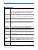
Table 2 lists some of the issues which may require attention.
Table 2. Model Upgrade Issues
Issue Action
PLL output clocks
cannot be named
In previous versions of DSP Builder, it was possible to have a PLL block and multiple
ClockAltr blocks which represented PLL outputs. The PLL output clocks took the names
of the clock blocks. This feature is not supported in v7.1 and cannot be automatically
fixed. In v7.1, the PLL output clocks are named <pll name>_clk<output index>. All
source blocks and rate change blocks referencing clock pins must be manually edited
to reference these PLL clock output pins.
PLL period multiply
and divide values
must be integers
In previous versions, the multiply and divide values could have non-integer values and
could be specified using MATLAB variables. In v7.1, you must specify the clock period
ratio directly as an integer period multiplier and an integer period divider. MATLAB
variables cannot be used.
The PLL output clock
period is incorrect
after upgrade
Occasionally, the PLL parameters are upgraded incorrectly. Open the PLL parameter
dialog and enter the correct values for the period multipliers and dividers.
When upgrading a
design with a PLL,
extra clock blocks are
created for each
distinct sample time
The extra Clock and Clock_Derived blocks should be removed, and any blocks
referencing them manually corrected to reference the PLL-driven clocks. Note that the
numbering of these clock pins will not in general match the numbering of the PLL clocks.
The PLL input clock
frequency information
is lost during the
upgrade process
Typically, you may want to create a new Clock block replicating this information, as the
base clock pin generated by the upgrade script is unlikely to be the correct driving clock
domain. For example, if the PLL specified an input clock frequency of 50 MHz, add a
Clock block and configure it to a clock period of 20ns and sample time 20e-9.
Clock blocks do not
support rate change
divider
In previous versions, the ClockAltr blocks supported a rate change option (Addition
Clock Divider) which could be used to generate a slower clock signal. This feature is not
supported in v7.1. If you want to generate different frequency clocks internally in 7.1,
you must add a PLL block driven from the required input clock.
Error assigning clock
for Dual-Clock FIFO
block
Under some circumstances - noted by the message “No clock specified for {write/read}
port, ...” you may have to manually select clocks after upgrading designs containing the
Dual-Clock FIFO block.
Error assigning PLL
clock for Multi-Rate
DFF block
When upgrading a Multi-Rate DFF block connected to a PLL clock, an error is issued of
the form: “Cannot upgrade clock in block foo/Multi-Rate DFF. Original clock source: PLL
CLOCK0.” The blocks must be manually corrected to reference the PLL clock.
Unnecessary clock
specification for
source blocks
In general, source blocks do not need to specify a clock domain, if it can be inferred from
the blocks they are driving. However, the upgrade path always specifies a clock if it is
not the base clock. Your multi-clock design may be easier to maintain if, after upgrading,
you manually turn off Specify Clock for source blocks – especially constant, VCC and
GND blocks – wherever possible.
Errors issued if a
constant, GND or
VCC block is driving a
block with a different
sample time
These errors can usually be fixed by turning off Specify Clock on the constant block. If
the block is fed into several clock domains, you also need to add a Tsamp block before
each one.