
Specifications


FC protocol, version 2, HC9S08 implementation
Developer’s Serial Bootloader, Rev. 13
Freescale Semiconductor 19
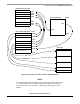
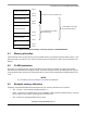
Figure 16. Simplified example of memory allocation in MC9S08GB/GT60
4.1 Memory allocation
The bootloader code occupies the top-end of FLASH memory (the highest memory address space). This
placement allows an effective use of the FLASH protection technique (see MCU specific data sheet for
details).
4.2 FLASH protection
By setting a FLASH protection register, all address space above this address is protected from both
intentional and unintentional erasing/rewriting. After the bootloader and the FLASH protection register
are programmed into memory, the bootloader code is protected from unintentional modification by user
code.
NOTE
See FLASH protection technique not usable for limitations.
4.3 Example memory allocation
Examples of the MC9S08GB/GT60 bootloader to the PC memory allocation are as follows:
• $82 - Version 2, read command implemented (bit 7)
• $r002 - System device identification register (SDIDR) content ($002 for GB/GT Family, r (four top
bits) is chip revision number reflecting current silicon level
• $02 - Number of reprogrammable memory areas
INTERRUPT VECTOR TABLE
NONVOLATILE REGISTERS
BOOTLOADER CODE
FLASH 58772 BYTES
HIGH PAGE REGISTERS
FLASH 1920 BYTES
RAM
I/O REGISTERS
0xFFC0
0xFFFF
0xFFB0
0xFE00
0x182C
0x1800
0x1080
0x0080
0x0000
FLASH MEMORY AVAILABLE
FOR USER CODE
FLASH MEMORY AVAILABLE
ON MC9S08GB/GT60 MCU
THIS AREA OF FLASH IS PROTECTED
RELOCCTOR TABLE
0xFDC0