
Specifications


Developer’s Serial Bootloader, Rev. 13
FC protocol, version 2, HC9S08 implementation
Freescale Semiconductor18
with an external voltage, V
TST
, present on the IRQ pin (normal monitor mode). Because this feature is
completely dedicated to bootloader code protection, it is unavailable to the user application code. If the
value for FLPBR appears in the user S19 code, a warning is displayed. Such an occurrence should be
omitted from user S19 code.
Some families have the FLASH block protection register stored in RAM instead (the MC68HC908JK/JL
Families are like this). The bootloader sets the correct value at the beginning of its execution to protect
itself. However, user code can modify this register and protect its own memory areas as needed. This also
implies that the bootloader is not 100% protected from user code.
See the specific MCU data sheet for a detailed explanation.
3.5.5 SRS register unusable
The bootloader uses an SRS register (as described in User code start) to recognize the reset source to
determine whether the user code will run. Because the SRS register is one-time readable (that is, it is reset
after first read), the user code does not have access to the SRS register value (if the bootloader is present
in the memory and makes the first read after each reset). There is no simple solution for this situation. After
the SRS register is read by the bootloader, it is stored in one RAM location. Its memory location may differ
from one implementation to another. If the application requires the SRS register and bootloader, the user
must redirect the SRSR reading to this specific RAM location. This location can be obtained from the
bootloader’s MAP file.
4 FC protocol, version 2, HC9S08 implementation
This section describes features that are specific to the HC9S08 bootloader implementation. The memory
allocation is heavily MCU specific so the meaning of variables is explained in this section.
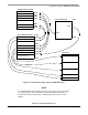
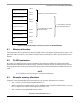
Figure 16 shows the memory allocation typical to the HC9S08 devices with the bootloader
preprogrammed. For example, the MC9S08GB/GT60 device memory map includes:
• 60 KB of FLASH memory ($1080–$17FF, $182C–$FFAF)
• 4 KB of random-access memory (RAM) ($0080–$107F)
• 16 bytes of nonvolatile registers ($FFB0–$FFBF)
• 64 bytes of user-defined vectors ($FFC0–$FFFF)