
Integrated Controller Hardware Specifications Sheet


88F6281
Hardware Specifications
Doc. No. MV-S104859-U0 Rev. E Copyright © 2008 Marvell
Page 88 Document Classification: Proprietary Information December 2, 2008, Preliminary
8.6.2 SDRAM DDR2 Interface AC Timing
8.6.2.1 SDRAM DDR2 Interface AC Timing Table
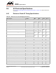
Table 46: SDRAM DDR2 Interface AC Timing Table
Min Max
Clock frequency fCK MHz -
DQ and DM valid output time before DQS transition tDOVB 0.40 - ns -
DQ and DM valid output time after DQS transition tDOVA 0.40 - ns -
DQ and DM output pulse w idth tDIPW 0.35 - tCK(avg) -
DQS output high pulse w idth tDQSH 0.35 - tCK(avg) -
DQS output low pulse w idth tDQSL 0.35 - tCK(avg) -
DQS falling edge to CLK-CLKn rising edge tDSS 0.34 - tCK(avg) 1
DQS falling edge from CLK-CLKn rising edge tDSH 0.34 - tCK(avg) 1
DQS latching rising transitions to associated clock edges tDQSS -0.11 0.11 tCK(avg) -
DQS w rite preamble tWPRE 0.35 - tCK(avg) -
DQS w rite postamble tWPST 0.40 - tCK(avg) -
Average CLK-CLKn high-level w idth tCH(avg) 0.48 0.52 tCK(avg) 1, 2, 3
Average CLK-CLKn low -level w idth tCL(avg) 0.48 0.52 tCK(avg) 1, 2, 4
DQ input setup time relative to DQS in transition tDSI -0.42 - ns -
DQ input hold time relative to DQS in transition tDHI 0.70 - ns -
Address and control output pulse w idth tIPW 0.60 - tCK(avg) -
Note s:
General comment: All timing values are defined from Vref to Vref, unless otherw ise specified.
General comment: All input timing values assume minimum slew rate of 1 V/ns (slew rate defined from Vref +/-125 mV).
General comment: tCK(avg) is calculated as the average clock period across any consecutive 200 cycle window .
General comment: All timing parameters w ith DQS signal are defined on DQS-DQSn crossing point.
General comment: For Address and Control output timing parameters, refer to the Address Timing table.
General comment: For all signals, the load is CL = 14 pF.
1. This timing value is defined on CLK / CLKn crossing point.
2. Refer to SDRAM DDR2 clock specifications table for more information.
3. tCH(avg) is defined as the average HIGH pulse w idth, as calculated across any consecutive 200 HIGH pulses.
4. tCL(avg) is defined as the average LOW pulse w idth, as calculated across any consecutive 200 LOW pulses.
400.0
Note sDe scription Sym bol
400 MHz @ 1.8V
Units