
Data Sheet
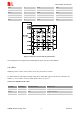

Smart Machine Smart Decision
SIM800F_Hardware Design_V1.00 50 2015-07-31
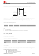
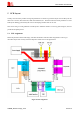
5.2 Principle of PCB Layout
During layout, we should pay attention to the following interfaces, such as Antenna, power supply, SIM card
interface, audio interface and so on.
5.2.1 Antenna
The length of trace between pin output and connector should be as short as possible
Do not trace RF signal over across the board
The RF signal should be far away from SIM card, power ICs
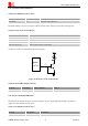
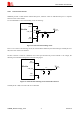
5.2.2. Power Supply
Not only VBAT but also return GND are very important in layout
The positive line of VBAT should be as short and wide as possible
The correct flow from source to VBAT pin should go though Zener diode then huge capacitor
Pin 36 and Pin37 are GND signals, and shortest layout to GND of power source should be designed
There are 10 GND pads in the module; these pads could enhance the GND performances. On the
upper layer of these pads, do not trace any signal if possible
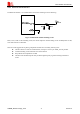
5.2.3 SIM Card Interface
SIM card holder has no anti-EMI component inside. Thus SIM card interface maybe interfered,
please pay more attention on this interface during layout
Ensure SIM card holder is far way from antenna or RF cable inside
Put SIM card holder near the module, as nearer as possible
Add ESD component to protect SIM_CLK, SIM_DATA, SIM_RST and SIM_VDD signals which
should be far away from power and high-speed-frequency signal
5.2.4 Audio Interface
The signal trace of audio should far away from antenna and power
The audio signal should avoid to parallel with VBAT trace
5.2.5 Others
It is better to trace signal lines of UART bunched, as well as signals of USB.