
Datasheet


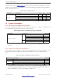


Table Of Contents
- Product Overview
- 1 ESP32-S3 Series Comparison
- 2 Pin Definition
- 3 Functional Description
- 3.1 CPU and Memory
- 3.2 RTC and Low-Power Management
- 3.3 Analog Peripherals
- 3.4 System Components
- 3.5 Digital Peripherals
- 3.5.1 IO MUX and GPIO Matrix
- 3.5.2 Serial Peripheral Interface (SPI)
- 3.5.3 LCD Interface
- 3.5.4 Camera Interface
- 3.5.5 UART Controller
- 3.5.6 I2C Interface
- 3.5.7 I2S Interface
- 3.5.8 Remote Control Peripheral
- 3.5.9 Pulse Count Controller
- 3.5.10 LED PWM Controller
- 3.5.11 USB 2.0 OTG Full-Speed Interface
- 3.5.12 USB Serial/JTAG Controller
- 3.5.13 Motor Control PWM (MCPWM)
- 3.5.14 SD/MMC Host Controller
- 3.5.15
- 3.6 Radio and Wi-Fi
- 3.7 Bluetooth LE
- 3.8 Timers and Watchdogs
- 3.9 Cryptography/Security Components
- 3.10 Peripheral Pin Configurations
- 4 Electrical Characteristics
- 5 Package Information
- 6 Related Documentation and Resources
- Revision History

4 Electrical Characteristics
In real-life applications, when VDD_SPI works in 3.3 V output mode, VDD3P3_CPU may be affected
by R
SP I
. For example, when VDD3P3_CPU is used to drive a 3.3 V flash, it should comply with the
following specifications:
VDD3P3_CPU > VDD_flash_min + I_flash_max*R
SP I
Among which, VDD_flash_min is the minimum operating voltage of the flash, and I_flash_max the
maximum current.
For more information, please refer to section 2.7 Power Scheme.
4.4 DC Characteristics (3.3 V, 25 °C)
Table 17: DC Characteristics (3.3 V, 25 °C)
Symbol Parameter Min Typ Max Unit
C
IN
Pin capacitance — 2 — pF
V
IH
High-level input voltage 0.75 × VDD
1
— VDD
1
+ 0.3 V
V
IL
Low-level input voltage –0.3 — 0.25 × VDD
1
V
I
IH
High-level input current — — 50 nA
I
IL
Low-level input current — — 50 nA
V
OH
2
High-level output voltage 0.8 × VDD
1
— — V
V
OL
2
Low-level output voltage — — 0.1 × VDD
1
V
I
OH
High-level source current (VDD
1
= 3.3 V, V
OH
>= 2.64 V, PAD_DRIVER = 3)
— 40 — mA
I
OL
Low-level sink current (VDD
1
= 3.3 V, V
OL
=
0.495 V, PAD_DRIVER = 3)
— 28 — mA
R
P U
Internal weak pull-up resistor — 45 — kΩ
R
P D
Internal weak pull-down resistor — 45 — kΩ
V
IH_nRST
Chip reset release voltage (CHIP_PU voltage is
within the specified range)
0.75 × VDD
1
— VDD
1
+ 0.3 V
V
IL_nRST
Chip reset voltage (CHIP_PU voltage is within
the specified range)
–0.3 — 0.25 × VDD
1
V
1
VDD is the I/O voltage for a particular power domain of pins.
2
V
OH
and V
OL
are measured using high-impedance load.
4.5 ADC Characteristics
Table 18: ADC Characteristics
Symbol Parameter Min Max Unit
DNL (Differential nonlinearity)
1
ADC connected to an external
–4 4 LSB
100 nF capacitor; DC signal input;
INL (Integral nonlinearity)
Ambient temperature at 25 °C;
–8 8 LSB
Wi-Fi off
Sampling rate — — 100 kSPS
2
1
To get better DNL results, you can sample multiple times and apply a filter, or calculate the average value.
2
kSPS means kilo samples-per-second.
Espressif Systems 52
Submit Documentation Feedback
ESP32-S3 Series Datasheet v1.2