ESP32S3 Series Datasheet 2.4 GHz WiFi + Bluetooth® LE SoC Supporting IEEE 802.11b/g/n (2.4 GHz WiFi) and Bluetooth® 5 (LE) Including: ESP32-S3 ESP32-S3FN8 ESP32-S3R2 ESP32-S3R8 ESP32-S3R8V ESP32-S3FH4R2 Version 1.2 Espressif Systems Copyright © 2022 www.espressif.
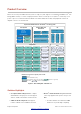
Product Overview ESP32-S3 is a low-power MCU-based system-on-chip (SoC) that supports 2.4 GHz Wi-Fi and Bluetooth® Low Energy (Bluetooth LE). It consists of high-performance dual-core microprocessor (Xtensa® 32-bit LX7), a low power coprocessor, a Wi-Fi baseband, a Bluetooth LE baseband, RF module, and peripherals. The block diagram of the SoC is shown below. Espressif’s ESP32-S3 Wi-Fi + Bluetooth® Low Energy SoC Wireless MAC and Baseband Wi-Fi MAC SRAM JTAG ROM Bluetooth LE Link Controller 2.
performance interfaces that allow connection to flash and external RAM – Efficient L1 cache to improve execution of • Reliable security features ensured by external memory – Single-precision floating-point unit (FPU) to – Cryptographic hardware accelerators that accelerate computing support AES-128/256, Hash, RSA, HMAC, digital signature, and secure boot • Highlyintegrated RF module that provides – Random number generator industry-leading power and RF performance • Stateoftheart power manageme
interfaces that allow connection to multiple flash • Analog interfaces: and external RAM – 2 × 12-bit SAR ADCs, up to 20 channels • Flash controller with cache is supported – 1 × temperature sensor • Flash in-Circuit Programming (ICP) is supported – 14 × touch sensing IOs • Timers: Advanced Peripheral Interfaces – 4 × 54-bit general-purpose timers • 45 × programmable GPIOs – 1 × 52-bit system timer • Digital interfaces: – 3 × watchdog timers – 4 × SPI – 1 × LCD interface (8-bit ~16-bit paralle
– Baby monitor – Internet radio players • Consumer Electronics • Generic Low-power IoT Sensor Hubs – Smart watch and bracelet • Generic Low-power IoT Data Loggers – Over-the-top (OTT) devices • Cameras for Video Streaming – Wi-Fi and bluetooth speaker • USB Devices – Logger toys and proximity sensing toys • Speech Recognition • Smart Agriculture • Image Recognition – Smart greenhouse • Wi-Fi + Bluetooth Networking Card – Smart irrigation • Touch Sensing – Agriculture robot – Waterproof de
Contents Contents Product Overview 2 Solution Highlights 2 Features 3 Applications 4 1 ESP32S3 Series Comparison 11 1.1 ESP32-S3 Series Nomenclature 11 1.2 Comparison 11 2 Pin Definition 12 2.1 Pin Layout 12 2.2 Pin Description 13 2.3 Pin Name Description 16 2.4 Function Name Description 16 2.5 GPIO Functions 17 2.6 Pin-to-Pin Mapping Between Chip and SiP Flash/PSRAM 19 2.7 Power Scheme 20 2.8 Strapping Pins 21 3 Functional Description 25 3.1 25 3.2 3.3 3.
Contents 3.4.8 Clock Glitch Detection 3.5 31 Digital Peripherals 32 3.5.1 IO MUX and GPIO Matrix 32 3.5.2 Serial Peripheral Interface (SPI) 32 3.5.3 LCD Interface 33 3.5.4 Camera Interface 34 3.5.5 UART Controller 34 3.5.6 I2C Interface 34 3.5.7 I2S Interface 35 3.5.8 Remote Control Peripheral 35 3.5.9 Pulse Count Controller 35 3.5.10 LED PWM Controller 36 3.5.11 USB 2.0 OTG Full-Speed Interface 36 3.5.12 USB Serial/JTAG Controller 37 3.5.13 Motor Control PWM (MCPWM) 37 3.5.
Contents 4.2 Recommended Operating Conditions 51 4.3 VDD_SPI Output Characteristics 51 4.4 DC Characteristics (3.3 V, 25 °C) 52 4.5 ADC Characteristics 52 4.6 Current Consumption 53 4.6.1 RF Current Consumption in Active Mode 53 4.6.2 Current Consumption in Other Modes 53 4.7 Reliability 55 4.8 Wi-Fi Radio 55 4.9 4.8.1 Wi-Fi RF Transmitter (TX) Specifications 55 4.8.2 Wi-Fi RF Receiver (RX) Specifications 56 Bluetooth LE Radio 57 4.9.
List of Tables List of Tables 1 ESP32-S3 Series Comparison 11 2 Pin Description 13 3 Pin Name Description 16 4 Function Name Description 16 5 GPIO Functions 17 6 Pin-to-Pin Mapping Between Chip and SiP Flash/PSRAM 19 7 Description of ESP32-S3 Power-up and Reset Timing Parameters 21 8 JTAG Signal Source Selection 22 9 Strapping Pins 22 10 The Default Value for VDD_SPI Voltage 23 11 Parameter Descriptions of Setup and Hold Times for the Strapping Pin 24 12 Connection Between
List of Figures List of Figures 1 Block Diagram of ESP32-S3 2 ESP32-S3 Series Nomenclature 11 3 ESP32-S3 Pin Layout (Top View) 12 4 ESP32-S3 Power Scheme 21 5 ESP32-S3 Power-up and Reset Timing 21 6 Setup and Hold Times for the Strapping Pin 23 7 Address Mapping Structure 26 8 QFN56 (7×7 mm) Package 62 Espressif Systems 2 10 Submit Documentation Feedback ESP32-S3 Series Datasheet v1.
1 ESP32-S3 Series Comparison 1. ESP32S3 Series Comparison 1.1 ESP32S3 Series Nomenclature ESP32-S3 F H x R x V 1.8 V external SPI flash only PSRAM size (MB) PSRAM Flash size (MB) Flash temperature H: High temperature N: Normal temperature Flash Chip series Figure 2: ESP32S3 Series Nomenclature 1.2 Comparison Table 1: ESP32S3 Series Comparison Ordering Code SiP Flash SiP PSRAM Ambient Temperature (°C) SPI Voltage — — –40 ∼ 105 3.3 V/1.8 V ESP32-S3FN8 8 MB (Quad SPI) — –40 ∼ 85 3.
2 Pin Definition 2. Pin Definition 43 GPIO38 44 MTCK 45 MTDO 46 VDD3P3_CPU 47 MTDI 48 MTMS 49 U0TXD 50 U0RXD 51 GPIO45 52 GPIO46 53 XTAL_N 54 XTAL_P 55 VDDA 56 VDDA 2.
2 Pin Definition Espressif Systems 2.2 Pin Description Table 2: Pin Description Name No. Type Power Domain Function LNA_IN 1 I/O — Low Noise Amplifier (RF LNA) input and output signal VDD3P3 2 PA — Analog power supply VDD3P3 3 PA — Analog power supply High: on, enables the chip. CHIP_PU 4 I VDD3P3_RTC Low: off, the chip powers off. Note: Do not leave the CHIP_PU pin floating. 13 Submit Documentation Feedback ESP32-S3 Series Datasheet v1.
Submit Documentation Feedback ESP32-S3 Series Datasheet v1.2 No.
No. Type Power Domain Function XTAL_P 54 — — External crystal input VDDA1 55 PA — Analog power supply VDDA2 56 PA — Analog power supply GND 57 G — Ground 1 P: power pin; PA : analog power pin; PD : digital power pin; I: input; O: output; T: high impedance. 2 Pin functions in bold font are the default pin functions in SPI Boot mode. For pins No.38 ∼ 42, the default function is decided by eFuse bit.
2 Pin Definition 2.3 Pin Name Description The explanation of each pin name is briefly described below. Table 3: Pin Name Description Pin Name Description General-purpose input and output (x is GPIO number). GPIO pins can GPIOx be assigned various functions, including digital and analog functions. For more information on digital functions, please refer to Table 5. SiP flash/PSRAM and external flash/RAM interface (x is CLK, CS0, CS1, SPIx D, Q, WP, HD, IO4~7 or DQS).
ESP32-S3 has 45 GPIO pins (numbering 22-25 is not used) which can be assigned various functions as listed in Table 5. The functions listed here are digital functions (F0-F4). RTC functions and analog functions can be found in Table 2. Table 5: GPIO Functions 17 Submit Documentation Feedback ESP32-S3 Series Datasheet v1.
Submit Documentation Feedback Pin Name F0 Type F1 Type F2 Type F3 Type F4 Type At Reset After Reset Notes 30 SPICLK SPICLK O/T GPIO30 I/O/T - - - - - - IE1, WPU1 IE1, WPU1 - 31 SPIQ SPIQ I1/O/T GPIO31 I/O/T - - - - - - IE1, WPU1 IE1, WPU1 - 32 SPID SPID I1/O/T GPIO32 I/O/T - - - - - - IE1, WPU1 IE1, WPU1 - 33 GPIO33 GPIO33 I/O/T GPIO33 I/O/T FSPIHD I1/O/T SUBSPIHD I1/O/T SPIIO4 I1/O/T IE0 IE1 - 34 GPIO34 GPIO34 I/O/T GPIO34
2 Pin Definition Type Each digital function (Fn, n=0~4) is associated with a “Type”. The description of “Type” is as follows: • O: Output only. • O/T: The signal can be output or high-impedance. • I/O/T: The signal can be input, output, and high-impedance. • I1: Input only. If the pin is assigned a function other than Fn, the input signal of Fn is always “1”. • I1/O/T: The signal can be input, output, and high-impedance. If Fn is not selected, the input signal of Fn is always “1”.
2 Pin Definition ESP32S3R2 / ESP32S3FH4R2 SiP PSRAM (2 MB, Quad SPI) SPICLK CLK SPICS1 CE# SPID SI/SIO0 SPIQ SO/SIO1 SPIWP SIO2 SPIHD SIO3 ESP32S3R8 / ESP32S3R8V SiP PSRAM (8 MB, Octal SPI) SPICLK CLK SPICS1 CE# SPID DQ0 SPIQ DQ1 SPIWP DQ2 SPIHD DQ3 GPIO33 DQ4 GPIO34 DQ5 GPIO35 DQ6 GPIO36 DQ7 GPIO37 DQS/DM 2.
2 Pin Definition The power scheme diagram is shown in Figure 4. Figure 4: ESP32S3 Power Scheme Notes on CHIP_PU: Figure 5 shows the power-up and reset timing of ESP32-S3 series. Details about the parameters are listed in Table 7. t0 t1 2.
2 Pin Definition • GPIO0 • GPIO45 • GPIO46 • GPIO3 Software can read the values of corresponding bits from register “GPIO_STRAPPING”. During the chip’s system reset (power-on-reset, RTC watchdog reset, brownout reset, analog super watchdog reset, and crystal clock glitch detection reset), the latches of the strapping pins sample the voltage level as strapping bits of “0” or “1”, and hold these bits until the chip is powered down or shut down.
2 Pin Definition Pin Default GPIO3 N/A EFUSE_DIS_USB_JTAG = 0, EFUSE_DIS_PAD_JTAG = 0, EFUSE_STRAP_JTAG_SEL=1 0: JTAG signal from on-chip JTAG pins 1: JTAG signal from USB Serial/JTAG controller Note: 1. The strapping combination of GPIO46 = 1 and GPIO0 = 0 is invalid and will trigger unexpected behavior. 2. By default, the ROM boot messages are printed over UART0 (U0TXD pin) and USB Serial/JTAG controller together. The ROM code printing can be disabled through configuration register and eFuse.
2 Pin Definition Table 11: Parameter Descriptions of Setup and Hold Times for the Strapping Pin Parameter Description tSU Setup time before CHIP_PU goes from low to high 0 tHD Hold time after CHIP_PU goes high 3 Espressif Systems Min (ms) 24 Submit Documentation Feedback ESP32-S3 Series Datasheet v1.
3 Functional Description 3. Functional Description This chapter describes the functional modules of ESP32-S3. 3.1 CPU and Memory 3.1.
3 Functional Description • External RAM mapped into 32 MB data space as individual blocks of 64 KB. 8-bit, 16-bit, 32-bit, and 128-bit reads and writes are supported. External flash can also be mapped into 32 MB data space as individual blocks of 64 KB, but only supporting 8-bit, 16-bit, 32-bit and 128-bit reads. Note: After ESP32-S3 is initialized, firmware can customize the mapping of external RAM or flash into the CPU address space. 3.1.
3 Functional Description • Instruction cache: 16 KB (one bank) or 32 KB (two banks) Data cache: 32 KB (one bank) or 64 KB (two banks) • Instruction cache: four-way or eight-way set associative Data cache: four-way set associative • Block size of 16 bytes or 32 bytes for both instruction cache and data cache • Pre-load function • Lock function • Critical word first and early restart 3.1.
3 Functional Description • Lightsleep mode: The CPU is paused. The RTC peripherals, as well as the ULP coprocessor can be woken up periodically by the timer. Any wake-up events (MAC, host, RTC timer, or external interrupts) will wake up the chip. Wireless connection can remain active. Users can optionally decide what peripherals to shut down/keep on (refer to Figure 1), for power-saving purpose. • Deepsleep mode: CPU and most peripherals are powered down.
3 Functional Description The temperature sensor has a range of –20 °C to 110 °C. It is designed primarily to sense the temperature changes inside the chip. The temperature value depends on factors such as microcontroller clock frequency or I/O load. Generally, the chip’s internal temperature is higher than the ambient temperature. 3.3.3 Touch Sensor ESP32-S3 has 14 capacitive-sensing GPIOs, which detect variations induced by touching or approaching the GPIOs with a finger or other objects.
3 Functional Description 3.4.3 Permission Control In ESP32-S3, the Permission Control module is used to control access to the slaves (including internal memory, peripherals, external flash and RAM). The host can access its slave only if it has the right permission. In this way, data and instructions are protected from illegitimate read or write. The ESP32-S3 CPU can run in both Secure World and Non-secure World where independent permission controls are adopted.
3 Functional Description Manual. 3.4.5 GDMA Controller ESP32-S3 has a general-purpose DMA controller (GDMA) with five independent channels for transmitting and another five independent channels for receiving. These ten channels are shared by peripherals that have DMA feature, and support dynamic priority. The DMA controller controls data transfer using linked lists. It allows peripheral-to-memory and memory-to-memory data transfer at a high speed. All channels can access internal and external RAM.
3 Functional Description For more information, please refer to Chapter Clock Glitch Detection in ESP32-S3 Technical Reference Manual. 3.5 Digital Peripherals 3.5.
3 Functional Description frequency is configurable. Data transmission is in multiples of bytes. The clock polarity (CPOL) and phase (CPHA) are also configurable. The SPI2 interface supports DMA. – In two-line full-duplex communication mode, the host’s clock frequency is configurable to 80 MHz at most, and the slave’s clock frequency to 60 MHz at most. Four modes of SPI transfer format are supported. Only SDR reads and writes are supported.
3 Functional Description 3.5.4 Camera Interface ESP32-S3 supports an 8-bit ~16-bit DVP image sensor, with clock frequency of up to 40 MHz. The camera interface supports conversion among RGB565, YUV422, YUV420, and YUV411. 3.5.5 UART Controller ESP32-S3 has three UART (Universal Asynchronous Receiver Transmitter) controllers, i.e., UART0, UART1, and UART2, which support IrDA and asynchronous communication (RS232 and RS485) at a speed of up to 5 Mbps.
3 Functional Description 3.5.7 I2S Interface ESP32-S3 includes two standard I2S interfaces. They can operate in master mode or slave mode, in full-duplex mode or half-duplex communication mode, and can be configured to operate with an 8-bit, 16-bit, 24-bit, or 32-bit resolution as an input or output channel. BCK clock frequency, from 10 kHz up to 40 MHz, is supported. The I2S interface has a dedicated DMA controller.
3 Functional Description Manual. 3.5.10 LED PWM Controller The LED PWM controller can generate independent digital waveforms on eight channels. The LED PWM controller has the following features: • Can generate a digital waveform with configurable periods and duty cycle. The duty cycle resolution can be up to 14 bits within a 1 ms period. • Has multiple clock sources, including APB clock and external main crystal clock. • Can operate when the CPU is in Light-sleep mode.
3 Functional Description – A control pipe consists of two channels (IN and OUT), as IN and OUT transactions must be handled separately. Only Control transfer type is supported. – Each of the other seven channels is dynamically configurable to be IN or OUT, and supports Bulk, Isochronous, and Interrupt transfer types. • All channels share an RX FIFO, non-periodic TX FIFO, and periodic TX FIFO. The size of each FIFO is configurable.
3 Functional Description • Up to 80 MHz clock output • Three data bus modes: – 1-bit – 4-bit (supports two SD/SDIO/MMC 4.41 cards, and one SD card operating at 1.8 V in 4-bit mode) – 8-bit For more information, please refer to Chapter SD/MMC Host Controller (SDHOST) in ESP32-S3 Technical Reference Manual. 3.5.
3 Functional Description 3.6.1 2.4 GHz Receiver The 2.4 GHz receiver demodulates the 2.4 GHz RF signal to quadrature baseband signals and converts them to the digital domain with two high-resolution, high-speed ADCs. To adapt to varying signal channel conditions, ESP32-S3 integrates RF filters, Automatic Gain Control (AGC), DC offset cancelation circuits, and baseband filters. 3.6.2 2.4 GHz Transmitter The 2.4 GHz transmitter modulates the quadrature baseband signals to the 2.
3 Functional Description 3.6.5 WiFi MAC ESP32-S3 implements the full 802.11 b/g/n Wi-Fi MAC protocol. It supports the Basic Service Set (BSS) STA and SoftAP operations under the Distributed Control Function (DCF). Power management is handled automatically with minimal host interaction to minimize the active duty period.
3 Functional Description • Simultaneous advertising and scanning • Multiple connections in simultaneous central and peripheral roles • Adaptive frequency hopping and channel assessment • LE channel selection algorithm #2 • Connection parameter update • High duty cycle non-connectable advertising • LE privacy 1.2 • LE data packet length extension • Link layer extended scanner filter policies • Low duty cycle directed advertising • Link layer encryption • LE Ping 3.8 Timers and Watchdogs 3.8.
3 Functional Description For more information, please refer to Chapter System Timer (SYSTIMER) in ESP32-S3 Technical Reference Manual. 3.8.3 Watchdog Timers The ESP32-S3 contains three watchdog timers: one in each of the two timer groups (called Main System Watchdog Timers, or MWDT) and one in the RTC Module (called the RTC Watchdog Timer, or RWDT). During the flash boot process, RWDT and the first MWDT are enabled automatically in order to detect and recover from booting errors.
3 Functional Description • Encryption and decryption functions jointly determined by registers configuration, eFuse parameters, and boot mode For more information, please refer to Chapter External Memory Encryption and Decryption (XTS_AES) in ESP32-S3 Technical Reference Manual. 3.9.2 Secure Boot Secure Boot feature uses a hardware root of trust to ensure only signed firmware (with RSA-PSS signature) can be booted. 3.9.
3 Functional Description 3.9.6 SHA Accelerator ESP32-S3 integrates an SHA accelerator, which is a hardware device that speeds up SHA algorithm significantly. The SHA Accelerator supports the following features: • All the hash algorithms introduced in FIPS PUB 180-4 Spec.
3 Functional Description 3.9.8 RSA Accelrator The RSA Accelerator provides hardware support for high precision computation used in various RSA asymmetric cipher algorithms.
3 Functional Description Interface Touch sensor JTAG Signal Pin TOUCH1 GPIO1 TOUCH2 GPIO2 TOUCH3 GPIO3 TOUCH4 GPIO4 TOUCH5 GPIO5 TOUCH6 GPIO6 TOUCH7 GPIO7 TOUCH8 GPIO8 TOUCH9 GPIO9 TOUCH10 GPIO10 TOUCH11 GPIO11 TOUCH12 GPIO12 TOUCH13 GPIO13 TOUCH14 GPIO14 MTDI MTDI MTCK MTCK MTMS MTMS MTDO MTDO Function Capacitive touch sensors JTAG for software debugging U0RXD_in U0CTS_in U0DSR_in U0TXD_out U0RTS_out U0DTR_out U1RXD_in U1CTS_in UART U1DSR_in Any GPIO pins U1T
3 Functional Description Interface Signal Pin Function I2S0O_BCK_in I2S0_MCLK_in I2S0O_WS_in I2S0I_SD_in I2S0I_SD1_in I2S0I_SD2_in I2S0I_SD3_in I2S0I_BCK_in I2S0I_WS_in I2S1O_BCK_in I2S1_MCLK_in I2S1O_WS_in I2S1I_SD_in I2S I2S1I_BCK_in Any GPIO pins I2S1I_WS_in Stereo input and output from/to the audio codec I2S0O_BCK_out I2S0_MCLK_out I2S0O_WS_out I2S0O_SD_out I2S0O_SD1_out I2S0I_BCK_out I2S0I_WS_out I2S1O_BCK_out I2S1_MCLK_out I2S1O_WS_out I2S1O_SD_out I2S1I_BCK_out I2S1I_WS_out LCD_PCLK LCD_DC
3 Functional Description Interface SPI0/1 Signal Pin Function SPICLK_out_mux SPICLK SPICS0_out SPICS0 SPICS1_out SPICS1 SPID_in/_out SPID SPIQ_in/_out SPIQ Support Standard SPI, Dual SPI, SPIWP_in/_out SPIWP QSPI, QPI, OSPI, and OPI that SPIHD_in/_out SPIHD allow connection to external flash SPID4_in/_out GPIO33 and RAM.
3 Functional Description Interface USB OTG Signal Pin Function D- GPIO19 (for internal PHY) D+ GPIO20 (for internal PHY) VP MTMS (for external PHY) VM MTDI (for external PHY) RCV GPIO21 (for external PHY) OEN MTDO (for external PHY) VPO MTCK (for external PHY) VMO GPIO38 (for external PHY) D- GPIO19 (for internal PHY) Full-speed USB OTG (USB OTG supports both full-speed on-chip PHY and external PHY) D+ GPIO20 (for internal PHY) Flash programming and CPU USB VP MTMS (for externa
3 Functional Description Interface Signal Pin Function PWM0_SYNC0~2_in PWM0_F0~2_in PWM0_CAP0~2_in PWM1_SYNC0~2_in PWM1_F0~2_in PWM1_CAP0~2_in Two MCPWM input and output PWM0_out0a pins.
4 Electrical Characteristics 4. Electrical Characteristics 4.1 Absolute Maximum Ratings Stresses beyond the absolute maximum ratings listed in the table below may cause permanent damage to the device. These are stress ratings only, and do not refer to the functional operation of the device.
4 Electrical Characteristics In real-life applications, when VDD_SPI works in 3.3 V output mode, VDD3P3_CPU may be affected by RSP I . For example, when VDD3P3_CPU is used to drive a 3.3 V flash, it should comply with the following specifications: VDD3P3_CPU > VDD_flash_min + I_flash_max*RSP I Among which, VDD_flash_min is the minimum operating voltage of the flash, and I_flash_max the maximum current. For more information, please refer to section 2.7 Power Scheme. 4.4 DC Characteristics (3.
4 Electrical Characteristics ESP-IDF provides couple of calibration methods for ADC. Results after calibration using hardware + software calibration are shown in Table 19. For higher accuracy, users may apply other calibration methods provided in ESP-IDF, or implement their own.
4 Electrical Characteristics Table 22: Current Consumption in Modemsleep Mode Frequency Work mode Description (MHz) WAITI (Dual core in idle state) 21.8 18.7 24.4 19.9 25.4 Dual core running 128-bit data access instructions 23.0 28.8 WAITI 22.0 36.1 28.4 42.6 33.1 47.3 35.1 49.6 Dual core running 128-bit data access instructions 41.8 56.3 WAITI 27.6 42.3 39.9 54.6 49.6 64.1 54.4 69.2 Dual core running 128-bit data access instructions 66.7 81.1 WAITI 32.9 47.6 51.
4 Electrical Characteristics 4.7 Reliability Table 23: Reliability Qualifications Test Item HTOL (High Temperature Operating Life) Test Conditions Test Standard 125 °C, 1000 hours JESD22-A108 HBM (Human Body Mode)1± 2000 V ESD (Electro-Static Discharge Sensitivity) JS-001 2 CDM (Charge Device Mode) ± 1000 V JS-002 Current trigger ± 200 mA Latch up JESD78 Voltage trigger 1.
4 Electrical Characteristics Table 25 – cont’d from previous page Min Typ Max (dBm) (dBm) (dBm) 802.11n, HT20, MCS7 — 18.5 — 802.11n, HT40, MCS0 — 19.5 — 802.11n, HT40, MCS7 — 18.0 — Rate Table 26: TX EVM Test Rate Min Typ SL1 (dB) (dB) (dB) 802.11b, 1 Mbps, @21 dBm — –24.5 –10 802.11b, 11 Mbps, @21 dBm — –24.5 –10 802.11g, 6 Mbps, @20.5 dBm — –21.5 –5 802.11g, 54 Mbps, @19 dBm — –28.0 –25 802.11n, HT20, MCS0, @19.5 dBm — –23.0 –5 802.11n, HT20, MCS7, @18.
4 Electrical Characteristics Table 27 – cont’d from previous page Min Typ Max (dBm) (dBm) (dBm) 802.11n, HT20, MCS6 — –75.8 — 802.11n, HT20, MCS7 — –74.2 — 802.11n, HT40, MCS0 — –90.0 — 802.11n, HT40, MCS1 — –88.0 — 802.11n, HT40, MCS2 — –85.2 — 802.11n, HT40, MCS3 — –82.0 — 802.11n, HT40, MCS4 — –79.0 — 802.11n, HT40, MCS5 — –74.4 — 802.11n, HT40, MCS6 — –72.8 — 802.11n, HT40, MCS7 — –71.
4 Electrical Characteristics Table 30: Bluetooth LE Frequency Parameter Center frequency of operating channel Min Typ Max (MHz) (MHz) (MHz) 2402 — 2480 4.9.1 Bluetooth LE RF Transmitter (TX) Specifications Table 31: Transmitter Characteristics Bluetooth LE 1 Mbps Parameter Description Min RF power control range RF transmit power Carrier frequency offset and drift Modulation characteristics In-band spurious emissions Typ Max Unit –25.00 0 20.00 Gain control step — 3.
4 Electrical Characteristics Table 33: Transmitter Characteristics Bluetooth LE 125 Kbps Parameter Description Min RF power control range RF transmit power Carrier frequency offset and drift Modulation characteristics Max Unit –25.00 0 20.00 Gain control step — 3.00 — dB Max |fn |n=0, 1, 2, ..k — 0.80 — kHz Max |f0 − fn | — 0.98 — kHz |fn − fn−3 | — 0.30 — kHz |f0 − f3 | — 1.00 — kHz ∆ f 1avg — 248.00 — kHz — 222.00 — kHz ±2 MHz offset — –37.
4 Electrical Characteristics Table 35 – cont’d from previous page Parameter Description Image frequency Adjacent channel to image frequency Out-of-band blocking performance Intermodulation Min Typ Max Unit F > F0 + 3 MHz — –32 — dB F > F0 – 3 MHz — –36 — dB — — –32 — dB F = Fimage + 1 MHz — –39 — dB F = Fimage – 1 MHz — –31 — dB 30 MHz ~ 2000 MHz — –9 — dBm 2003 MHz ~ 2399 MHz — –19 — dBm 2484 MHz ~ 2997 MHz — –16 — dBm 3000 MHz ~ 12.
4 Electrical Characteristics Table 37 – cont’d from previous page Parameter Description Image frequency Adjacent channel to image frequency Min Typ Max Unit F = F0 + 2 MHz — –32 — dB F = F0 – 2 MHz — –39 — dB F = F0 + 3 MHz — –35 — dB F = F0 – 3 MHz — –45 — dB F > F0 + 3 MHz — –35 — dB F > F0 – 3 MHz — –48 — dB — — –35 — dB F = Fimage + 1 MHz — –49 — dB F = Fimage – 1 MHz — –32 — dB Table 38: Receiver Characteristics Bluetooth LE 500 Kbps Parameter Des
5 Package Information 5. Package Information Pin 1 Pin 2 Pin 3 Pin 1 Pin 2 Pin 3 Figure 8: QFN56 (7×7 mm) Package Note: • The pins of the chip are numbered in an anti-clockwise direction from Pin 1 in the top view. • For information about tape, reel, and product marking, please refer to Espressif Chip-Packing Information. Espressif Systems 62 Submit Documentation Feedback ESP32-S3 Series Datasheet v1.
6 Related Documentation and Resources 6. Related Documentation and Resources Related Documentation • ESP32-S3 Technical Reference Manual – Detailed information on how to use the ESP32-S3 memory and peripherals. • ESP32-S3 Hardware Design Guidelines – Guidelines on how to integrate the ESP32-S3 into your hardware product. • Certificates https://espressif.com/en/support/documents/certificates • Documentation Updates and Update Notification Subscription https://espressif.
Revision History Revision History Date Version Release Notes • Updated description of ROM code printing in Section 2.8 2022-07 v1.2 • Updated Figure 1 • Update Section 4.6 • Deleted the hyperlinks in Application • Synchronized eFuse size throughout 2022-04 v1.
Revision History Date Version Release Notes • Added ”for chip revision 0” on cover, in footer and watermark to indicate that 2021-07-19 v0.5.1 the current and previous versions of this datasheet are for chip version 0 • Corrected a few typos 2021-07-09 v0.5 Espressif Systems Preliminary version 65 Submit Documentation Feedback ESP32-S3 Series Datasheet v1.
Disclaimer and Copyright Notice Information in this document, including URL references, is subject to change without notice. ALL THIRD PARTY’S INFORMATION IN THIS DOCUMENT IS PROVIDED AS IS WITH NO WARRANTIES TO ITS AUTHENTICITY AND ACCURACY. NO WARRANTY IS PROVIDED TO THIS DOCUMENT FOR ITS MERCHANTABILITY, NONINFRINGEMENT, FITNESS FOR ANY PARTICULAR PURPOSE, NOR DOES ANY WARRANTY OTHERWISE ARISING OUT OF ANY PROPOSAL, SPECIFICATION OR SAMPLE.