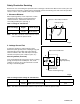
SERVICE MANUAL Main Section I Specifications I Preparation for Servicing I Adjustment Procedures I Schematic Diagrams I CBA’s I Exploded Views I Parts List When servicing the deck mechanism, refer to MK14 Deck Mechanism Section. Deck Mechanism Part No.: N2466FT This service manual is for the MWC24T5 version B model, which is different from the previous model. For MWC24T5 version B model, a suffix “B” is printed on the rating label on the back of the unit. Refer to the rating label illustration at right.
IMPORTANT SAFETY NOTICE Proper service and repair is important to the safe, reliable operation of all Funai Equipment. The service procedures recommended by Funai and described in this service manual are effective methods of performing service operations. Some of these service special tools should be used when and as recommended.
MAIN SECTION 24″ COLOR TV/DVD/VCR MWC24T5 Main Section I Specifications I Preparation for Servicing I Adjustment Procedures I Schematic Diagrams I CBA’s I Exploded Views I Parts List TABLE OF CONTENTS Specifications . . . . . . . . . . . . . . . . . . . . . . . . . . . . . . . . . . . . . . . . . . . . . . . . . . . . . . . . . . . . . . . . . . . . . . . . . . 1-1-1 Laser Beam Safety Precautions . . . . . . . . . . . . . . . . . . . . . . . . . . . . . . . . . . . . . . . . . . . . . . . . . . . . . . .
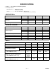
SPECIFICATIONS *ˆ Mode---------SP mode unless otherwise specified * Test input terminal --------Video input (1 Vp-p) Audio input (-10 dB) ------------------Ant. input (80 dBµV) Video: 87.5% Audio: 25 kHz dev. (1 kHz Sin) < DEFLECTION > Description Condition Unit Nominal Limit --- % 90 5 Horizontal % --- ±18 Vertical % --- ±10 --- kV 27 --- Condition Unit Nominal Limit Center m/m --- 0.4 Corner m/m --- 2.5 Side m/m --- 1.5 2.
< VCR > Description Condition Unit Nominal Limit 1. Horizontal Resolution (R/P, SP) Line 230 200 2. Jitter (Low) (R/P, SP) µs 0.1 0.2 AM(SP) (R/P, SP) dB 38 33 PM(SP) (R/P, SP) dB 38 33 (R/P, SP) % 0.25 0.5 Condition Unit Nominal Limit 1. Video S/N (80 dBµV, TV4ch) --- dB 45 40 2. Audio S/N (W/LPF) --- dB 45 40 3. S/N Chroma 4. Wow & Flutter (JIS, UNWTD) < TUNER > Description < NORMAL AUDIO> All items are measured across 8 Ω resistor at speaker output terminal.
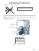
LASER BEAM SAFETY PRECAUTIONS This DVD player uses a pickup that emits a laser beam. Do not look directly at the laser beam coming from the pickup or allow it to strike against your skin. The laser beam is emitted from the location shown in the figure. When checking the laser diode, be sure to keep your eyes at least 30 cm away from the pickup lens when the diode is turned on. Do not look directly at the laser beam.
IMPORTANT SAFETY PRECAUTIONS Prior to shipment from the factory, our products are strictly inspected for recognized product safety and electrical codes of the countries in which they are to be sold. However, in order to maintain such compliance, it is equally important to implement the following precautions when a set is being serviced. Safety Precautions for TV Circuit AC line cord directly into a 120 V AC outlet. (Do not use an isolation transformer during this test.
an isolation transformer only if the AC power plug is inserted so that the chassis is connected to the ground side of the AC power source. To confirm that the AC power plug is inserted correctly, with an AC voltmeter, measure between the chassis and a known earth ground. If a voltage reading in excess of 1.0V is obtained, remove and reinsert the AC power plug in the opposite polarity and again measure the voltage potential between the chassis and a known earth ground.
2) Strip about 15 mm of the insulation from the ends of the wires. If the wires are stranded, twist the strands to avoid frayed conductors. of the countries in which they are to be sold. However, in order to maintain such compliance, it is equally important to implement the following precautions when a set is being serviced. 3) Align the lengths of the wires to be connected. Insert the wires fully into the connector. Precautions during Servicing A.
Safety Check after Servicing Examine the area surrounding the repaired location for damage or deterioration. Observe that screws, parts and wires have been returned to original positions. Afterwards, perform the following tests and confirm the specified values in order to verify compliance with safety standards. 1. Clearance Distance When replacing primary circuit components, confirm specified clearance distance (d) and (d') between soldered terminals, and between terminals and surrounding metallic parts.
STANDARD NOTES FOR SERVICING Circuit Board Indications Pb (Lead) Free Solder 1. The output pin of the 3 pin Regulator ICs is indicated as shown. Pb free mark will be found on PCBs which use Pb free solder. (Refer to figure.) For PCBs with Pb free mark, be sure to use Pb free solder. For PCBs without Pb free mark, use standard solder. Top View Out Bottom View In Input 2. For other ICs, pin 1 and every fifth pin are indicated as shown. 5 Pb free mark Pin 1 How to Remove / Install Flat Pack-IC 10 3.
around the flat pack-IC to protect other parts from damage. (Fig. S-1-2) 3. The flat pack-IC on the CBA is affixed with glue, so be careful not to break or damage the foil of each pin or the solder lands under the IC when removing it. With Soldering Iron: 1. Using desoldering braid, remove the solder from all pins of the flat pack-IC. When you use solder flux which is applied to all pins of the flat pack-IC, you can remove it easily. (Fig.
With Iron Wire: 2. Installation 1. Using desoldering braid, remove the solder from all pins of the flat pack-IC. When you use solder flux which is applied to all pins of the flat pack-IC, you can remove it easily. (Fig. S-1-3) 1. Using desoldering braid, remove the solder from the foil of each pin of the flat pack-IC on the CBA so you can install a replacement flat pack-IC more easily. 2. Affix the wire to a workbench or solid mounting point, as shown in Fig. S-1-5. 2.
Instructions for Handling Semiconductors Electrostatic breakdown of the semi-conductors may occur due to a potential difference caused by electrostatic charge during unpacking or repair work. 1. Ground for Human Body Be sure to wear a grounding band (1 MΩ) that is properly grounded to remove any static electricity that may be charged on the body. 2.
PREPARATION FOR SERVICING How to Enter the Service Mode Key Adjustment Mode 7 Purity check mode: Shows Red, Green, Blue or White cyclically on the screen each time the [7] button is pressed. 8 H. Position adjustment: See adjustment instructions page 1-7-5. 9 V. Shift/V.Size adjustment: See adjustment instructions page 1-7-5. Caution 1: 1. Optical sensors system are used for Tape Start and End Sensor on this equipment.
CABINET DISASSEMBLY INSTRUCTIONS 1. Disassembly Flowchart Removal This flowchart indicates the disassembly steps for the cabinet parts, and the CBA in order to gain access to item(s) to be serviced. When reassembling, follow the steps in reverse order. Bend, route and dress the cables as they were. Step/ Loc. No. Part CAUTION! [8] Deck Assembly When removing the CRT, be sure to discharge the Anode Lead of the CRT with the CRT Ground Wire before removing the Anode Cap.
Reference Notes in the Table 1) Disconnect Connector (CN301) on the DVD Main CBA Unit. CAUTION! 2) Short the three short lands of FPC cable with solder before removing the FFC cable (CN201) from it. If you disconnect the FFC cable (CN201), the laser diode of pickup will be destroyed. (Fig. D4) When removing the CRT, be sure to discharge the Anode Lead of the CRT with the CRT Ground Wire before removing the Anode Cap. 1.
[2] Tray Chassis Unit (S-5) (S-7) Top Shield (S-5) (S-7) [4] DVD Mechanism (S-8) (S-8) (S-6) (S-6) (S-6) (S-8) [8] Deck Assembly [5] DVD Main CBA Unit [6] Sub CBA (S-11) (S-11) (S-11) [7] Function CBA [9] Main CBA (S-9) (S-10) Fig.
Anode Cap (S-4) CRT CBA (S-4) (S-4) [3] CRT (S-4) Fig. D3 A DVD Mechanism Short the three short lands by soldering. (Either of two places.) FPC Cable View for A Fig.
DVD MAIN CBA UNIT CN301 CN201 JUNCTION-B CBA TO SPEAKER CN1A CN2A CL3801 CN3801 ANODE CN2801 FUNCTION CBA CRT GND CN2571 CN1 CL2601 CN2503 CN2502 SUB CBA CN2 CN2401 FOCUS CL2501A MAIN CBA CL2504A CN1803 CL1403 CN1301 CN1602 CL1401 SCREEN CRT CBA CN2501 CL2501B CL1402 CN1601 AC CORD CN1802 CL1201 TUNER CN3802 CL3802 ACE HEAD ASSEMBLY TO SPEAKER JUNCTION-A CBA FE HEAD DECK ASSEMBLY CYLINDER ASSEMBLY CAPSTAN MOTOR Fig.
ELECTRICAL ADJUSTMENT INSTRUCTIONS General Note: “CBA” is abbreviation for “Circuit Board Assembly.” Note: Electrical adjustments are required after replacing circuit components and certain mechanical parts. It is important to perform these adjustments only after all repairs and replacements have been completed. Also, do not attempt these adjustments unless the proper equipment is available. How to enter the Service mode: Service mode: 1. Use the service remote control unit. 2. Turn the power on.
2. Setting for CONTRAST, COLOR, TINT, V-TINT and SHARP Data Values 3. H f0 Adjustment General Symptom of Misadjustment: Horizontal position and size of screen image may not be properly displayed. 1. Enter the Service mode. (See page 1-7-1.) Purpose: To get correct horizontal position and size of screen image. 2. Press [PICTURE] button on the service remote control unit. Display changes “BRT,” “CNT,” “COL,” “TNT,” “V-T,” and “SHP” cyclically when [PICTURE] button is pressed. Test Point Adj.
4. Cut-off Adjustment 5. H. Size Adjustment Purpose: To adjust the beam current of R, G, B, and screen voltage. Symptom of Misadjustment: White color may be reddish, greenish or bluish. Test Point Adj. Point Mode Input --- Screen-Control [CH. o / p] buttons RF Black Raster Tape M. EQ. Spec. --- Pattern Generator See Reference Notes below. Purpose: To obtain correct size of screen image. Symptom of Misadjustment: Size of screen image may not be properly displayed. Test point Adj.
7. White Balance Adjustment 8. Sub-Brightness Adjustment Purpose: To mix red, green and blue beams correctly for pure white. Purpose: To get proper brightness. Symptom of Misadjustment: White becomes bluish or reddish. Symptom of Misadjustment: If Sub-Brightness is incorrect, proper brightness cannot be obtained by adjusting the Brightness Control. Test Point Adj. Point Mode Input Test Point Adj. Point Mode Input Screen [CH. o / p] buttons RF White Raster (APL 100%) --- [CH.
9. Focus Adjustment 11. V. Shift Adjustment Purpose: Set the optimum Focus. Purpose: To obtain correct vertical position of screen image. Symptom of Misadjustment: If Focus Adjustment is incorrect, blurred images are shown on the display. Test Point Adj. Point Mode Input --- Focus Control --- Monoscope Tape M. EQ. Spec. --- Pattern Generator See below Symptom of Misadjustment: If V. position is incorrect, vertical position of image on the screen may not be properly displayed.
13. Head Switching Position Adjustment Purpose: Determine the Head Switching Position during Playback. The following 2 adjustments normally are not attempted in the field. They should be done only when replacing the CRT then adjust as a preparation. 14. Purity Adjustment Symptom of Misadjustment: May cause Head Switching Noise or Vertical Jitter in the picture. Purpose: To obtain pure color. Note: Unit reads Head Switching Position automatically and displays it on the screen (Upper Left Corner).
15. Convergence Adjustment 4. Fix the C.P. Magnets by tightening the Ring Lock. Purpose: To obtain proper convergence of red, green and blue beams. 5. Remove the DY Wedges and slightly tilt the Deflection Yoke horizontally and vertically to obtain the best overall convergence. Symptom of Misadjustment: If Convergence Adjustment is incorrect, the edge of white letters may have color edges. 6. Fix the Deflection Yoke by carefully inserting the DY Wedges between CRT and Deflection Yoke. Test Point Adj.
HOW TO INITIALIZE THE TV/DVD/VCR To put the program back at the factory-default, initialize the TV/DVD/VCR as the following procedure. < DVD Section > < TV/VCR Section > 1. Turn the power on and press [SELECT] button on the remote control unit to put the TV/DVD/VCR into DVD mode. 1. Use the service remote control unit. 2. Press [1], [2], [3], [4], and [DISPLAY] buttons on the remote control unit in that order. Fig. a appears on the screen. 3.
FIRMWARE RENEWAL MODE 1. Turn the power on and press [SELECT] button on the remote control unit to put the TV/DVD/VCR into DVD mode. Then remove the disc on the tray. (It is possible to move to F/W version up mode only when the TV/DVD/VCR is in DVD mode with the tray open.) "*******" differs depending on the models. F/W Version Up Mode (*2) VERSION : Completed SUM : 7ABC Model No : ******* VERSION : *.** ************.ab7 2.
TO DVD SYSTEM CONTROL/SERVO BLOCK DIAGRAM CN1A SUB CBA BUFFER Q2202 Q2203 BUFFER 1-10-1 DRUM MOTOR M LOADING MOTOR PG SENSOR CYLINDER ASSEMBLY CONTROL HEAD ACE HEAD ASSEMBLY (DECK ASSEMBLY) 18 16 17 19 CN1 SDATA SCLK CS DVD-REMOTE FUNCTION CBA CN2401 5 KEY1 M CN1301 13 14 15 CN1803 5 M CAPSTAN MOTOR MOTOR DRIVE CIRCUIT AL+5V 6 7 8 9 10 11 12 5 RESET Q1205 +26V T-REEL Q1206 M+12V P-ON+5V(3) TIMER+5V CL1201 1 2 3 4 AL+5V TP1202 CTL-AMP-OUT SW1212 AL+5V LD-SW WF
1-10-2 JK1701 YCA-SCL YCA-SDA YCA-CS DV-SYNC CYLINDER ASSEMBLY VIDEO (R)-2 HEAD VIDEO (L)-2 HEAD VIDEO (L)-1 HEAD VIDEO (R)-1 HEAD (DECK ASSEMBLY) TO SYSTEM CONTROL/SERVO BLOCK DIAGRAM VIDEO-IN TO TV PROCESS BLOCK DIAGRAM VIDEO TU-VIDEO EXT-V-IN WF4 LINE TUNER VIDEO AGC 53 SERIAL 54 I/F 55 24 DV-SYNC 30 32 Q1401 BUFFER 1 2 3 4 5 6 Y/C MIX TO SYSTEM CONTROL/SERVO BLOCK DIAGRAM CL1401 VIDEO(R)-1 VIDEO-COM1 VIDEO(L)-1 VIDEO(L)-2 VIDEO-COM2 VIDEO(R)-2 R P FBC QV/QH 6dB AMP IC1401 (V
1-10-3 CN2 3 4 9 1 WF20 JK2701 TO Hi-Fi AUDIO BLOCK DIAGRAM TO SYSTEM CONTROL/SERVO BLOCK DIAGRAM CN2503 19 DVD-AUDIO(R) 18 DVD-AUDIO(L) 16 DVD-AUDIO-MUTE FULL ERASE HEAD FE HEAD AUDIO ERASE HEAD AUDIO HEAD ACE HEAD ASSEMBLY AUDIO-OUT(R) AUDIO-OUT(L) N-A-IN N-A-OUT SP-MUTE DVD-AUDIO-MUTE DVD-H VOLUME DIGITAL AUDIO-OUT (COXIAL) Q2619 SUB CBA MAIN CBA Q2701 BUFFER (DECK ASSEMBLY) TO DVD AUDIO BLOCK DIAGRAM CN2A CL1402 AUDIO-PB/REC AUDIO-COM AE-H AE-H/FE-H CL1403 1 FE-H 2 FE
1-10-4 NOR SW L-CH INSEL 6 7 N-A-OUT TO AUDIO BLOCK DIAGRAM R-CH INSEL 13 48 14 47 STEREO PLL PILOT DET L-CH PNR R-CH PNR 63 P R R P SW NOISE LIM LIM NOISE SW PILOT CANCEL STEREO FILTER 62 SAP DEMOD SAP FILTER SIF DEMOD 69 JK1702 57 AUDIO(L)-IN AUDIO(R)-IN JK1703 TO TV PROCESS SIF BLOCK DIAGRAM CONT SAP DET IC1701 (MTS/ SAP/ Hi-Fi AUDIO PROCESS/ Hi-Fi HEAD AMP) DEV DEV COMP VCO NOISE DET HOLD PULSE VCO COMP L-R DEMOD MAIN CBA LPF MATRIX LPF ST/SAP SW L-CH
TO SYSTEM CONTROL/SERVO BLOCK DIAGRAM 1 3 2 5 IF 7 AGC SDA SCL FSC TU1001 1-10-5 9 8 OSD-R OSD-G OSD-B OSD-BLK WF16 V-SYNC 59 WF15 H-SYNC 58 16 12 11 10 13 Q1403 BUFFER VCO V-SYNC PROCESS CIRCUIT H-SYNC PROCESS CIRCUIT INTELLIGENT MONITORING 6 SYNC SEPARATION SERIAL I/F 14 15 31 RF AGC 14 AFT VIDEO DET 4 IF AGC DET 4.
1-10-6 +B +B +26V CN2503 8 1 7 2 9 CN2502 1 2 6 CN2503 5 RED 4 GREEN 3 BLUE V-DRIVE H-DRIVE AFC ACL V-RAMP-NF TO TV PROCESS BLOCK DIAGRAM CN1301 TO TV PROCESS BLOCK DIAGRAM CN1301 TO POWER SUPPLY BLOCK DIAGRAM CN1602 CL2601 4 3 2 2 3 4 CL2504A RED GREEN BLUE WF10 H.DRIVE Q2591 SUB CBA Q2571 TP2504 GND TP2501 +B H.OUTPUT 4 5 3 1 Q2503 RED AMP T2572A WF12 6 9 7 10 8 6 AMP 11 S F Q2533 WF13 TP2506 AFC Q2501 BLUE AMP CL2501B 1 3 VR2530 PINC. Q2532 Q2530, Q2531 H.
L1601 LINE FILTER PS1601 F1601 4A/125V DG601 DEGAUSSING CN1601 COIL W1601 4A 125V D1606 BRIDGE RECTIFIER D1603 Q1602 1-10-7 RL1601 Q1605 VR1601 +B ADJ 4A 125V COLD Q1603 FEED Q1604 BACK 2 3 13 14 15 16 12 17 1 IC1601 ERROR VOLTAGE DET 9 8 6 11 10 4 HOT SWITCHING Q1601 3 T1601 CAUTION ! Fixed voltage (or Auto voltage selectable) power supply circuit is used in this unit.
1-10-8 SLED MOTOR M M SPINDLE MOTOR TRAY-IN TS(+) TS(-) DRIVE CBA TO DIGITAL SIGNAL PROCESS BLOCK DIAGRAM FS(+) FS(-) SP(+) SP(-) TRAY-IN GND SL(-) SL(+) CN301 6 5 1 4 3 2 + SLED MOTOR DRIVE 17 18 8 7 5 6 10 9 1 3 2 IC202 (OP AMP) - DVD MAIN CBA UNIT +3.
FS PICK-UP UNIT TS DETECTOR C D A B CD/DVD FS(+) FS(-) TS(+) TS(-) CD-LD DVD-LD PD-MONI GND(DVD-PD) GND(CD-PD) GND(LD) SDRAM 13 42 53 CN201 2 3 1 4 CD 4 6 FS(+) FS(-) TS(+) TS(-) IC201 (SW) DVD 159 DATA RAM INST.
SCHEMATIC DIAGRAMS / CBA’S AND TEST POINTS Standard Notes WARNING Many electrical and mechanical parts in this chassis have special characteristics. These characteristics often pass unnoticed and the protection afforded by them cannot necessarily be obtained by using replacement components rated for higher voltage, wattage, etc.
LIST OF CAUTION, NOTES, AND SYMBOLS USED IN THE SCHEMATIC DIAGRAMS ON THE FOLLOWING PAGES: 1. CAUTION: FOR CONTINUED PROTECTION AGAINST RISK OF FIRE, REPLACE ONLY WITH SAME TYPE_A,_V FUSE. ATTENTION: UTILISER UN FUSIBLE DE RECHANGE DE MÊME TYPE DE_A,_V. 2. CAUTION: Fixed Voltage (or Auto voltage selectable) power supply circuit is used in this unit.
Main 1/6 & Sensor Schematic Diagram < TV/VCR Section > 1-11-3 T2202SCM1
Main 2/6 Schematic Diagram < TV/VCR Section > 1-11-4 T2202SCM2
Main 3/6 Schematic Diagram < TV/VCR Section > 1-11-5 T2202SCM3
Main 4/6 Schematic Diagram < TV/VCR Section > 1-11-6 T2202SCM4
Main 5/6 & Junction-A Schematic Diagram < TV/VCR Section > 1-11-7 T2202SCM5
Main 6/6 Schematic Diagram < TV/VCR Section > CAUTION ! Fixed voltage (or Auto voltage selectable) power supply circuit is used in this unit. If Main Fuse (F1601) is blown , check to see that all components in the power supply circuit are not defective before you connect the AC plug to the AC power supply. Otherwise it may cause some components in the power supply circuit to fail. 4A 125V CAUTION ! : For continued protection against risk of fire, replace only with same type 4 A, 125V fuse.
Sub 1/2 Schematic Diagram < TV/VCR Section > 1-11-9 T2202SCSUB1
Sub 2/2 Schematic Diagram < TV/VCR Section > 1-11-10 T2202SCSUB2
CRT Schematic Diagram < TV/VCR Section > T2202SCCRT Function & Junction-B Schematic Diagram < TV/VCR Section > T2202SCF 1-11-11
DVD Main 1/3 Schematic Diagram < DVD Section > 1-11-12 T2202SCD1
DVD Main 2/3 Schematic Diagram < DVD Section > 1-11-13 T2202SCD2
DVD Main 3/3 Schematic Diagram < DVD Section > 1-11-14 T2202SCD3
Main CBA Top View < TV/VCR Section > Because a hot chassis ground is present in the power supply circuit, an isolation transformer must be used. Also, in order to have the ability to increase the input slowly,when troubleshooting this type power supply circuit, a variable isolation transformer is required. 4A 125V CAUTION ! : For continued protection against risk of fire, replace only with same type 4 A, 125V fuse. ATTENTION : Utiliser un fusible de rechange de même type de 4A, 125V.
Main CBA Bottom View < TV/VCR Section > Because a hot chassis ground is present in the power supply circuit, an isolation transformer must be used. Also, in order to have the ability to increase the input slowly,when troubleshooting this type power supply circuit, a variable isolation transformer is required. 4A 125V CAUTION ! : For continued protection against risk of fire, replace only with same type 4 A, 125V fuse. ATTENTION : Utiliser un fusible de rechange de même type de 4A, 125V.
Sub CBA Top View < TV/VCR Section > TP2504 GND VR2530 PIN C.
Sub CBA Bottom View < TV/VCR Section > WF19 PIN18 OF CN2503 WF17 TP2513 DVD-Y WF18 TP2512 DVD-C WF10 Q2571 Collector 1-11-18 WF11 PIN 5 CN2571 WF20 PIN2 OF CN2 BT1200F01023-A
CRT CBA Top View < TV/VCR Section > CRT CBA Bottom View < TV/VCR Section > WF12 Q2503 Collector 1-11-19 WF13 Q2502 Collector WF14 Q2501 Collector BT1200F01023-B
Function CBA Top View < TV/VCR Section > Junction-A CBA Top View < TV/VCR Section > Junction-A CBA Bottom View < TV/VCR Section > BT1200F01023-D Junction-B CBA Top View < TV/VCR Section > Junction-B CBA Bottom View < TV/VCR Section > Function CBA Bottom View < TV/VCR Section > BT1200F01023-E BT1200F01023-C 1-11-20
Upper: WF6 Lower: WF1 1DIV: 0.2V 2DIV: 5V 5ms TP1403 ENV. WF7 1DIV: 0.5V 0.5ms IC1401 PIN10 WF8 1DIV: 0.5V 0.5ms IC1401 PIN9 WF3 1DIV: 1V 10ms TP1202 CTL-AMP-OUT WF4 1DIV: 0.25V 20 µs IC1401 Pin 32 WF5 1DIV: 0.5V 20 µs TP1401 V-OUT WF2 1DIV: 0.2V 0.1µs IC1401 Pin 49 WF1 1DIV: 2V 5ms TP1402 RF-SW 1-12-1 WF16 1DIV: 1V 5ms IC1201 PIN 59 1V 0.1 0.1µsec WF20 1DIV: 1V 0.1µs CN2 PIN 1 SPDIF WF19 1DIV: 0.5V 0.
M M FULL ERASE HEAD FE HEAD ACE HEAD ASSEMBLY CONTROL HEAD AUDIO HEAD AUDIO ERASE HEAD CYLINDER ASSEMBLY VIDEO (R)-1 HEAD VIDEO (L)-1 HEAD VIDEO (L)-2 HEAD VIDEO (R)-2 HEAD Hi-FiAUDIO(R) HEAD Hi-FiAUDIO(L) HEAD DRUM MOTOR PG SENSOR LOADING MOTOR CAPSTAN MOTOR CL1402 AE-H AE-H/FE-H AUDIO-COM AUDIO-PB/REC CTL(+) CTL(-) CL1401 Hi-Fi-AUDIO(L) Hi-Fi-COM Hi-Fi-AUDIO(R) VIDEO(R)-2 VIDEO-COM2 VIDEO(L)-2 VIDEO(L)-1 VIDEO-COM1 VIDEO(R)-1 CL1201 CM+12V P-ON+5V(3) C-FG CM-F/R C-CONT FG-GND LD-CONT
SLED MOTOR SPINDLE MOTOR DVD MECHANISM M M 1-13-2 PICK UP UNIT DETECTOR 7 9 11 2 3 6 5 4 DRIVE CBA TRAY-IN TS FS 1 2 3 4 5 6 7 8 9 10 11 12 13 14 15 16 17 18 19 20 6 5 4 3 2 1 CN201 TS(+) FS(+) FS(-) TS(-) GND(CD-PD) GND(DVD-PD) PD-MONI DVD-LD GND(LD) CD-LD GND NU VREF NU B C A D CD/DVD P-ON+5V CN301 SP(+) SP(-) GND SL(-) SL(+) TRAY-IN DVD MAIN CBA UNIT CN2A SPDIF GND DVD-AUDIO(R) DVD-AUDIO(L) GND DVD-C GND DVD-Y DVD-AUDIO-MUTE DVD-ON+5V(NU) CN1A EV+1.2V EV+1.2V EV+1.
SYSTEM CONTROL TIMING CHARTS < TV/VCR Section > Mode SW: LD-SW LD-SW Position detection A/D Input voltage Limit (Calculated voltage) Symbol 3.76 V ~ 4.50 V (4.12 V) EJ 4.51 V ~ 5.00 V (5.00 V) CL 0.00 V ~ 0.25 V (0.00 V) SB 1.06 V ~ 1.50 V (1.21 V) TL 0.66 V ~ 1.05 V (0.91 V) FB 1.99 V ~ 2.60 V (2.17 V) SF 1.51 V ~ 1.98 V (1.80 V) SM 3.20 V ~ 3.75 V (3.40 V) AU 0.26 V ~ 0.65 V (0.44 V) AL 4.51 V ~ 5.00 V (5.00 V) SS 2.61 V ~ 3.19 V (2.
Chart 1 1) SP MODE 18 RF-SW The first rise of RF-SW after a rise in F-AD signal.
Chart 2 2) LP/EP MODE 18 RF-SW The first rise of RF-SW after a rise in F-AD signal.
Chart 3 EJ POWER -OFF 0.2S ST-S/ END-S "OFF" CASS.LOAD CL SB LD-FWD 0.2S SB 0.2S STOP(B) +100mS(NTSC) +620mS(PAL) TL 0.2S LD-FWD 1.2S 0.2S POWER FB TL 0.2S STOP 0.4S SM SF 0.2S 0.2S 0.2S LD-FWD SF SM AL AU LD-REV 0.5S SM 40mS 0.4S AU LD-REV 20mS 0.2S STOP(A) AL AU 0.2S 0.2S PLAY 0.8S 0.3S PLAY SS LD-FWD REW RS RS 0.3S RS1(RS2) 0.2S AL SS AU LD-REV FF FS LD-FWD AL 1.0S FS1(FS2) PLAY PLAY PLAY STILL (SLOW) SS AL LD-REV PLAY AU 0.2S 0.
Chart 4 SM FB SM SF LD-FWD FF SF REV 1.0S AU SM STOP 0.4S LD-REV 40mS SM AL AU 0.5S LD-FWD STOP(A) LD-REV SF TL FB REW 20mS 0.2S 0.2S FB SM SF LD-FWD REW SF LD-FWD LD-REV 40mS 0.4S SM AL AU SM AU 0.5S STOP 0.2S STOP(A) REC AU AL 0.2S 1.0S 20mS LD-FWD REC LD-FWD SS RS 2.5S Short REV LD-REV AL AU SS 0.2S REC PAUSE LD-FWD AL 1.2S 1.5S SS RS REC PAUSE REC or PAUSE REC STOP /EJECT LD-FWD REC LD-REV AU SM 1.5S(NTSC) 1.0S(PAL) 0.4S AL 0.2S LD-FWD 0.
< DVD Section > Tray Close ~ Play / Play ~ Tray Open Tray Close Tray IN (TL221) Disc Rotation Play Disc Stop Tray Open 3.3V 0V Sled Drive (TP303) 1.65V 0V Disc Drive (TP301) 1.65V 0V Focus Drive (TP304) 1.65V 0V Tracking Drive (TP302) 1.
IC PIN FUNCTION DESCRIPTIONS IC1201 (TV/VCR Micro Controller IC) “H” ≥ 4.5 V, “L” ≤ 1.0 V Pin IN/ No. OUT Signal Name 1 IN LD-SW 2 OUT DVD-LED Pin IN/ No.
Pin IN/ No.
LEAD IDENTIFICATIONS 2SK3561 MID-32A22F 2SA1175(F) 2SA950-O(TE2 F T) 2SC2120-O(TE2 F T) 2SC1627-Y(TE2.F.
EXPLODED VIEWS Cabinet SHINWHA TAPE SGT-730 (BLACK) Details for L551 and surrounding parts V501-2 SHINWHA TAPE SGT-730 (WHITE) L1 V501-1 A2 L1 A3 L551 Scotch Tape #880 B4 L2 CRT CBA B2 Scotch Tape #880 L3-1 TB18 B5 CLN551 L1 L1 B2 B2 DVD Mechanical Parts TL4 TL3 TB2 TL4 B4 L3-2 TL3 B4 1B2 B5 B1 Scotch Tape #880 V501 DL2 A1-1 B2 TL1-2 B4 L4 TL1-1 DB2 DG601 SP801 TL1-2 B6 TL1-1 DVD Main CBA Unit 1B1 TB3 TL1-2 Junction-B CBA Sub CBA A1-8 A1X TB17 TL1-3 TB19 A1-
Packing X2 X3 X4 S2 S7 Packing Tape Tape S6 X1 S3 S4 FR ON T S1 1-17-2 T2203PEX
MECHANICAL PARTS LIST PRODUCT SAFETY NOTE: Products marked with a # have special characteristics important to safety. Before replacing any of these components, read carefully the product safety notice in this service manual. Don't degrade the safety of the product through improper servicing. NOTE: Parts that are not assigned part numbers (---------) are not available. Ref. No. A1X Description FRONT CABINET ASSEMBLY T2202UC Part No.
ELECTRICAL PARTS LIST PRODUCT SAFETY NOTE: Products marked with a # have special characteristics important to safety. Before replacing any of these components, read carefully the product safety notice in this service manual. Don't degrade the safety of the product through improper servicing. Ref. No. C1212 NOTES: 1. Parts that are not assigned part numbers (---------) are not available. 2. Tolerance of Capacitors and Resistors are noted with the following symbols. C.....±0.25% D.....±0.5% F.....±1% G..
Ref. No. Description Ref. No. Part No. Description Part No. C1428 CHIP CERAMIC CAP.(1608) B K 0.01µF/50V CHD1JK30B103 C1764 ELECTROLYTIC CAP. 100µF/10V M H7 CE1AMAVSL101 C1429 ELECTROLYTIC CAP. 47µF/6.3V M H7 CE0KMAVSL470 C1766 ELECTROLYTIC CAP. 2.2µF/50V M H7 CE1JMAVSL2R2 C1430 CHIP CERAMIC CAP.(1608) B K 0.01µF/50V CHD1JK30B103 C1769 ELECTROLYTIC CAP. 22µF/16V M H7 CE1CMAVSL220 C1431 CHIP CERAMIC CAP. F Z 1µF/10V CHD1AZ30F105 C1770 CHIP CERAMIC CAP.
Ref. No. Description Part No. Ref. No. Description Part No. D1224 LED SIR-563ST3F P QPQPS1R563ST IC1401 IC Y/C/A LA71205M-MPB-E QSZBA0RSY037 D1229 ZENER DIODE MTZJT-7715B QDTB00MTZJ15 IC1601# PHOTOCOUPLER LTV-817C-F NPEC0LTV817F D1230 ZENER DIODE MTZJT-7715B QDTB00MTZJ15 IC1682# IC VOLTAGE REGULATOR 5V KIA7805API/P NSZBA0SJY041 D1231 ZENER DIODE MTZJT-7718A QDTA00MTZJ18 IC1701 IC HIFI LA72670BM-MPB-E QSZBA0RSY039 D1237 ZENER DIODE MTZJT-776.
Ref. No. Description Part No. R1202 CHIP RES. 1/16W G 22k Ω R1203 CHIP RES. 1/16W G 470 Ω RRXAGR5Z0471 R1204 CHIP RES. 1/16W G 1.5k Ω RRXAGR5Z0152 R1205 CHIP RES. 1/16W G 3.6k Ω RRXAGR5Z0362 R1206 CHIP RES. 1/16W G 10k Ω R1207 Ref. No. Description Part No. CHIP RES. 1/10W J 100k Ω RRXAJR5Z0104 R1284 CHIP RES. 1/10W J 220k Ω RRXAJR5Z0224 R1285 CHIP RES. 1/10W J 3.3k Ω RRXAJR5Z0332 R1286 CHIP RES. 1/10W J 3.3k Ω RRXAJR5Z0332 RRXAGR5Z0103 R1287 CHIP RES.
Ref. No. R1608 Description CARBON RES. 1/4W J 180k Ω Ref. No. Part No. Description Part No. RCX4JATZ0184 R1772 CHIP RES. 1/10W J 47k Ω RRXAJR5Z0473 R1609# CARBON RES. 1/4W J 1.5 Ω RCX4JATZ01R5 R1773 CHIP RES. 1/10W J 47k Ω RRXAJR5Z0473 R1610 CARBON RES. 1/4W J 1.8k Ω RCX4JATZ0182 R1774 CHIP RES. 1/10W J 22k Ω RRXAJR5Z0223 R1613 CARBON RES. 1/4W J 150 Ω RCX4JATZ0151 R1780 CHIP RES. 1/10W J 6.8k Ω RRXAJR5Z0682 R1614 CARBON RES. 1/4W J 1.2k Ω RCX4JATZ0122 R1781 CHIP RES.
Ref. No. TL6 Description SCREW B-TIGHT D3X8 BIND HEAD+ Ref. No. Part No. Description Part No. GBJB3080 C2560 FILM CAP.(P) 0.033µF/100V J CMA2AJS00333 CE1EMASDL470 TP1202 PCB JUMPER D0.6-P16.0 JW16.0T C2561 ELECTROLYTIC CAP. 47µF/25V M TP1301 PCB JUMPER D0.6-P9.0 JW9.0T C2573# FILM CAP.(P) 0.033µF/100V J CMA2AJS00333 TP1302 PCB JUMPER D0.6-P8.0 JW8.0T C2574# ELECTROLYTIC CAP. 4.7µF/250V M CE2EMASDL4R7 TP1303 PCB JUMPER D0.6-P8.5 JW8.5T C2577 FILM CAP.(P) 0.
Ref. No. Description Part No. L2701 PCB JUMPER D0.6-P5.0 JW5.0T Q2201 TRANSISTOR 2SC2785(F) QQSF02SC2785 Q2202 TRANSISTOR 2SC2785(F) QQSF02SC2785 TRANSISTORS Ref. No. Description Part No. R2564 CARBON RES. 1/4W J 3.3 Ω RCX4JATZ03R3 R2565# CARBON RES. 1/4W J 1 Ω RCX4JATZ01R0 R2566# CARBON RES. 1/4W J 1 Ω RCX4JATZ01R0 R2567# CARBON RES. 1/4W J 1.2 Ω RCX4JATZ01R2 Q2203 TRANSISTOR 2SC2785(F) QQSF02SC2785 R2568# CARBON RES. 1/4W J 1.
Ref. No. Description Part No. R3568# CARBON RES. 1/4W J 1.2 Ω RCX4JATZ01R2 R3576 CARBON RES. 1/4W J 150 Ω RCX4JATZ0151 R3580 PCB JUMPER D0.6-P5.0 JW5.0T FUNCTION CBA Ref. No. Description FUNCTION CBA (MPS-C) Consists of the following: MISCELLANEOUS Part No.
MWC24T5 T2202UC 2006-04-06