
User`s guide


Understanding the IBIS Model
i.MX53 System Development User’s Guide, Rev. 1
3-8 Freescale Semiconductor
3.6.1 [Model Selector] ddr
This model has the following parameters: voltage, mode of operation, drive strength, ODT enable/disable.
Mode of operation Controlled by the IOMUXC_SW_PAD_CTL_GRP_DDR_TYPE[26:25] register
in IOMUXC (IOMUX controller) DDR_SEL bits.
Drive strength Controlled by bits 21–19 (DSE) of the following registers in IOMUXC (IOMUX
controller): IOMUXC_SW_PAD_CTL_GRP_ADDDS,
IOMUXC_SW_PAD_CTL_GRP_B0DS,
IOMUXC_SW_PAD_CTL_GRP_B1DS,
IOMUXC_SW_PAD_CTL_GRP_CTLDS,
IOMUXC_SW_PAD_CTL_GRP_B2DS,
IOMUXC_SW_PAD_CTL_GRP_B3DS,
IOMUXC_SW_PAD_CTL_PAD_DRAM_SDODT0,
IOMUXC_SW_PAD_CTL_PAD_DRAM_SDODT
ODT enable Controlled by bits [18:16], [14:12], [10:8], and [6:4] in ODTCTRL in ESDCTL.
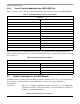
Example 3-5. [Model Selector] ddr in IBIS File
ddr2hs_sel00_ds111_mio DDR, 1.8V, ddr2 mode, 43 Ohm driver impedance
ddr2hs_sel00_ds110_mio DDR, 1.8V, ddr2 mode, 50 Ohm driver impedance
ddr2hs_sel00_ds101_mio DDR, 1.8V, ddr2 mode, 60 Ohm driver impedance
Refer to the register description in the IOMUXC chapter in the i.MX53 reference manual for further details
about this model.
3.6.2 [Model Selector] gpio
This model has the following parameters: voltage, drive strength, slew rate.
Drive strength Controlled by the DSE bits (bits 2–1) in the
IOMUXC_SW_PAD_CTL_PAD_<pad name>.
Slew rate Controlled by the SRE bit (bit 0) in the IOMUXC_SW_PAD_CTL_PAD_<pad
name>.
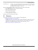
Example 3-6. [Model Selector] gpio in IBIS File
[Model Selector] gpio
gpio_iods0hvf GPIO, 2.775V, Low Drive, Fast SR
gpio_iods0hvs GPIO, 2.775V, Low Drive, Slow SR
gpio_iods0lvf GPIO, 1.875V, Low Drive, Fast SR
gpio_iods0lvs GPIO, 1.875V, Low Drive, Slow SR
Refer to the register description in the IOMUXC chapter in the i.MX53 reference manual for further details
about this model.