
User`s guide
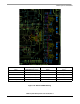


i.MX53 Layout Recommendations
i.MX53 System Development User’s Guide, Rev. 1
Freescale Semiconductor 2-29
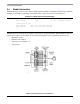
• USB_OTG_RREFEXT
•SATA_REXT
• LVDS_BG_RES
• TVDAC_VREF
• DRAM_CALIBRATION
Freescale recommends the use of a resistor of 1% tolerance or better with a connection that is made
through a short trace. The resistance of the connecting trace should be as low as possible (< 1 Ω). The
ground return should be short and direct to the ground plane.
NOTE
The reference resistor and the connection should be placed away from noisy
regions. Noise induced on it may impact the internal circuit and degrade the
interface signals.
2.11 ESD and Radiated Emissions Recommendations
The PCB design should use 6 or more layers, with solid power and ground planes and the
recommendations for ESD immunity and radiated emissions performance are as follows:
• All components with ground chassis shields (USB jack, buttons, etc.) should connect the shield to
the PCB chassis ground ring.
• Ferrite beads should be placed on each signal line connecting to an external cable. These ferrite
beads must be placed as close to the PCB jack as possible.
NOTE
Ferrite beads should have a minimum impedance of 500 Ω at 100 MHz with
the exception of the ferrite on USB_5V.
• Ferrite beads should NOT be placed on the USB D+/D– signal lines as this can cause USB signal
integrity problems. For radiated emissions problems due to USB, a common mode choke may be
placed on the D+/D– signal lines. However, in most cases, it should not be required if the PCB
layout is satisfactory. Ideally, the common mode choke should be approved for high speed USB
use or tested thoroughly to verify there are no signal integrity issues created.
• It is highly recommended that ESD protection devices be used on ports connecting to external
connectors. Refer to the reference schematic (available on the Freescale website) for detailed
information about ESD protection implementation on the USB and TV-E interfaces.