
User`s guide


i.MX53 Layout Recommendations
i.MX53 System Development User’s Guide, Rev. 1
2-26 Freescale Semiconductor
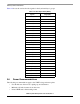
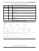
Table 2-4 shows the total etch of the signals for the byte 0 and byte 1 groups.
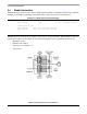
2.6 Power Recommendations
The following recommendations apply to the VREF voltage reference plane.
• Use 30 mils trace between de coupling cap and destination.
• Maintain a 25 mils clearance from other nets.
• Isolate VREF and/or shield with ground.
Table 2-4. Total Signal Etch (DDR3)
Signals Length (Mils)
DRAM_D0 616.034
DRAM_D1 612.886
DRAM_D2 613.808
DRAM_D3 612.701
DRAM_D4 617.177
DRAM_D5 614.486
DRAM_D6 614.743
DRAM_D7 613.145
DRAM_DQM0 612.794
DRAM_SDQS0 615.633
DRAM_SDQS0_B 614.36
DRAM_D8 615.063
DRAM_D9 611.525
DRAM_D10 616.758
DRAM_D11 614.928
DRAM_D12 614.521
DRAM_D13 612.822
DRAM_D14 612.794
DRAM_D15 614.369
DRAM_DQM1 614.705
DRAM_SDQS1 610.26
DRAM_SDQS1_B 617.892
DRAM_SDCLK0 1172.235
DRAM_SDCLK0_B 1174.757
DRAM_SDCLK1 1176.5
DRAM_SDCLK1_B 1175.963