
User`s guide

i.MX53 Layout Recommendations
i.MX53 System Development User’s Guide, Rev. 1
Freescale Semiconductor 2-9
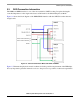
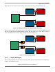
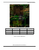
If the data bus is two byte groups by memory, the topology is fly-by, as shown in Figure 2-10.
Figure 2-10. Topology for Data Bus of Two Byte Groups by Memory
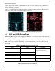
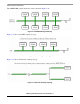
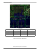
Figure 2-11 shows the clock routing topology. Clock routing uses a fly-by topology. The i.MX53 provides
two sets of clocks that are identical in timing and drive. This allows the user to select either clock pair to
route to the DDR devices. Thus, routing and clock loading is minimized.
Figure 2-11. Clock Routing Topology
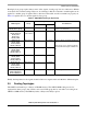
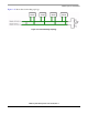
2.5.2 2 Gbyte Topologies
The following diagrams show the 2 Gbyte topologies. This option has eight memories and requires the
addition of a termination resistor.
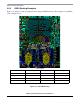
DDR Top
DDR Top
DDR Bottom
DDR Bottom
i.MX53
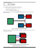
DDR Top
DDR Top
DDR Bottom
DDR Bottom
i.MX53