
User`s guide

i.MX53 Layout Recommendations
i.MX53 System Development User’s Guide, Rev. 1
Freescale Semiconductor 2-7
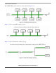
Routing by byte group requires better control of the signals of each group. It is also a little more difficult
for analysis and constraint settings. However, its advantage is that the constraint to match lengths can be
applied to a smaller group of signals. This is often more achievable once the constraints are properly set.
Table 2-2 explains how to route the signals by byte group.
Finally, the impedance for the signals should be 50 Ω for singled ended and 100 Ω for differential pairs.
2.5 Routing Topologies
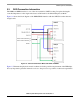
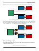
The i.MX53 can handle up to 2 Gbytes of DRAM memory. The i.MX53 DDR routing needs to be
separated into three groups: data, address, and control. Each group has its own method of routing from
i.MX53 to DDR memory. The DDR layout has 1 Gbyte and 2 Gbyte options.
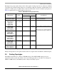
Table 2-2. DDR2/DDR3 Routing by Byte Group
i.MX53 Signals Group
Length
Considerations
Min Max
DRAM_SDCLK[1:0]
DRAM_SDCLK_B[1:0]
Clock Short as possible 2 inches Match the signals ± 5 mils.
2 inches is recommended.
DRAM_A[15:0]
DRAM_SDBA[2:0]
DRAM_RAS
DRAM_CAS
DRAM_SDWE
Address
and Command
Clock (min) – 200 Clock (min)
1
Match the signals ± 25 mils.
DRAM_D[7:0]
DRAM_DQM0
DRAM_SDQS0
DRAM_SDQS0_B
Byte Group 1 — Clock (min) Match the signals of each byte group ± 25
mils.
All byte groups (1 to 4) matched ± 50 mils
Match the differential signals of DQS ± 10
mils.
DRAM_D[15:8]
DRAM_DQM1
DRAM_SDQS1
DRAM_SDQS1_B
Byte Group 2 — Clock (min)
DRAM_D[23:16]
DRAM_DQM2
DRAM_SDQS2
DRAM_SDQS2_B
Byte Group 3 — Clock (min)
DRAM_D[31:24]
DRAM_DQM3
DRAM_SDQS3
DRAM_SDQS3_B
Byte Group 4 — Clock (min)
DRAM_CS[1:0]
DRAM_SDCKE[1:0]
DRAM_SDODT[1:0]
Control signals Clock (min) – 200 Clock (min) Match the signals ± 50 mils.
1
Clock (min)—The shortest length of the clock group signals because this group has a ± 5 mil matching tolerance.