
User`s guide

i.MX53 Layout Recommendations
i.MX53 System Development User’s Guide, Rev. 1
Freescale Semiconductor 2-3
2.1.1 Fanout
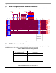
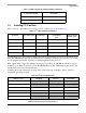
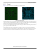
Figure 2-3 shows the fanouts for the i.MX53 for two different layers.
Figure 2-3. i.MX53 Fanouts
The fanout scheme creates a four quadrant structure that facilitates the placement of decoupling capacitors
on the bottom side of the PCB. This keeps them closer to the power balls, which is critical for minimizing
inductance and ensuring high-speed transient current demand by the processor.
A correct via size is critical for preserving adequate routing space. The recommended geometry for the via
pads is: pad size 16 mils and drill 8 mils.
The constraints for the trace size may depend on a number of factors, such as the board stackup and
associated di-electric and copper thickness, required impedance, and required current (for power traces).
On the Freescale reference design, the minimum trace width of 3 mils is used for the DDR routing.