
User`s guide

Design Checklist
i.MX53 System Development User’s Guide, Rev. 1
1-8 Freescale Semiconductor
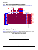
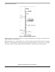
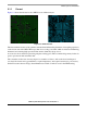
1.1 Boot Configuration Bus Isolation Resistors
Figure 1-1 shows the boot configuration bus isolation resistors referenced in recommendation 3.
Figure 1-1. Boot Configuration Bus Isolation Resistors
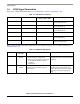
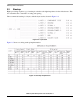
1.2 DDR Reference Circuit
Table 1-2 is a resistor chart (see recommendation 1). The recommendations are appropriate for designs
with DDR memory chips with a maximum Vref input current of 2 μA each.
Table 1-2. DDR Vref Resistor Sizing Guideline
Number of DRAM Packages with
2 μA Vref Input Current
Resistor Divider Value
(2 resistors)
21.21 kΩ 1%
2 1.54 kΩ 0.5%
2 2.32 kΩ 0.1%
4 768 Ω 1%
SW4_3V3
SW4_3V3
R2
0
R4
0
R8
0
R9
0
Bus
Isolation
Resistors
R11
0
R1
0
DNP
R3
0
DNP
R10
0
R5
0
DNP
R13
0
DNP
R12
0
DNP
R7
0
DNP
BT_CFG1_0
R6
0
DNP
IMX_LDO_1V8
EIM_A21
EIM_A20
EIM_A19
EIM_A18
EIM_A17BT_CFG1_2
BT_CFG1_3
EIM_A16
EIM_LBA
EIM_A22BT_CFG1_7
BT_CFG3_3
BT_CFG3_2
BT_CFG1_6
BT_CFG1_5
BT_CFG2_6
BT_CFG2_5
BT_CFG2_4
BT_CFG2_3
BT_CFG2_2
BT_CFG3_5
BT_CFG3_4
BT_CFG1_4
BT_CFG1_1
BT_CFG2_7
EIM_DA8
EIM_DA9
EIM_DA10
BT_CFG3_7
BT_CFG3_6
R344.7K
BT_CFG3_1
EIM_DA6
EIM_DA7
R264.7K
R144.7K
R364.7K
R174.7K
R204.7K
R214.7K
R154.7K
R184.7K
R314.7K
R234.7K
R254.7K
R334.7K
R354.7K
R274.7K
R194.7K
R164.7K
R304.7K
EIM_DA5
R324.7K
R224.7K
EIM_DA4
EIM_EB1
EIM_DA0
EIM_DA1
EIM_DA2
EIM_DA3
R244.7K
EIM_EB0
EI M_LBA
EIM_DA3
EIM_DA2
EIM_DA1
EIM_DA6
EIM_DA4
EIM_DA0
R291.0K
EIM_DA5
EIM_DA9
EIM_DA8
EIM_DA7
BOOT_MODE1
R281.0K
EI M_A 17
EI M_E B1
EIM_DA10
EI M_A 20
EI M_A 19
EI M_A 18
BOOT_MODE0
BOOT_MODE1
BOOT_MODE0
EI M_A 21
EI M_A 22
EI M_A 16
EI M_E B0
SW4_3V3
S1
SW _DI P- 10/S M
1
2
3
4
5
6
7
8
9
18
17
16
15
14
13
12
1110
19
20
RN 3 10K
1
2
3
4
5
6
7
8
9
10
RN 1 10K
1
2
3
4
5
6
7
8
9
10
RN 2 10K
1
2
3
4
5
6
7
8
9
10
GN D