
User`s guide


Design Checklist
i.MX53 System Development User’s Guide, Rev. 1
Freescale Semiconductor 1-3
JTAG Recommendations
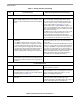
9. Do not use external pull-up or pull-down resistors on
JTAG_TDO.
JTAG_TDO is configured with an on-chip keeper circuit
such that the floating condition is eliminated if an external
pull resistor is not present. An external pull resistor on
JTAG_TDO is detrimental.
See Ta ble 1 -5 for a summary of the JTAG interface.
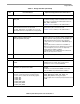
10.Ensure that the on-chip pull-up/down configuration is
followed If external resistors are used with
non-JTAG_TDO signals. For example, do not use an
external pull-down on an input that has on-chip pull-up.
External resistors can be used with non-JTAG_TDO
signals, but they do not need to be used.
See Ta ble 1 -5 for a summary of the JTAG interface.
Clock Amplifier (CAMP) Recommendations
11. After initialization, disable unused clock amplifiers
(CAMPs) within the CCM registers
(CCM_CCR[CAMPx_EN] field).
CKIH1 and CKIH2 are inputs feeding CAMPs (clock
amplifiers) that have on-chip AC coupling, eliminating the
need for external coupling capacitors. The CAMPs are
enabled by default, but the main clocks feeding the
on-chip clock tree are sourced from XTAL/EXTAL upon
power up.
Using low jitter external oscillators to feed CKIH1 or
CKIH2 is not required, but it can advantageous if low jitter
or special frequency clock sources are required by
modules driven by CKIH1 or CKIH2.
See CCM chapter in the i.MX53 Reference Manual for
details on the respective clock trees.
12. Tie CKIH1/CKIH2 to GND if they are unused. If disabled, the on-chip CAMP output is low.
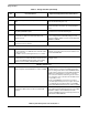
TVDAC Recommendations
13. Tie TVDAC_VREF to an external 1.05 kΩ 1% resistor
to GND.
TVDAC_VREF determines the Triple Video DAC
(TVDAC) reference voltage. This resistor must be
mounted close to the associated BGA ball.
14. Bypass the TVDAC_COMP reference with an
external 0.1 µF capacitor tied to GND.
This capacitor must be mounted close to the associated
BGA ball.
If TV OUT is not used, float the COMP contact and
ensure the DACs are powered down by software.
15. External ESD (electro-static discharge) and EOS
(electrical overstress) protection is required at the
processor device contacts for the following signals:
• TVDAC_IOB
• TVDAC_IOG
• TVDAC_IOR
• TVCDC_IOB_BACK
• TVCDC_IOG_BACK
• TVCDC_IOR_BACK
TVDAC_IOB, TVDAC_IOG, TVDAC_IOR,
TVCDC_IOB_BACK, TVCDC_IOG_BACK, and
TVCDC_IOR_BACK are analog TV outputs.
If the TV outputs are not used, they may be floated or tied
to GND.
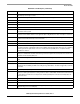
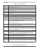
Table 1-1. Design Checklist (continued)
Check
Box
Recommendation Explanation/Supplemental Recommendations