
User`s guide


i.MX53 System Development User’s Guide, Rev. 1
Freescale Semiconductor 1-1
Chapter 1
Design Checklist
This chapter provides a design checklist for i.MX53-based systems. The design checklist contains
recommendations for optimal design. Where appropriate, the checklist also provides an explanation so that
users have a greater understanding of why certain techniques are recommended. All supplemental tables
referenced by the checklist appear following the design checklist table.
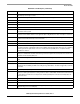
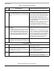
Table 1-1. Design Checklist
Check
Box
Recommendation Explanation/Supplemental Recommendations
DDR Recommendations
1. Tie DDR_VREF to a precision external resistor divider
with a resistor to GND and a resistor to
NVCC_EMI_DRAM.
When using DDR, the nominal reference voltage must be
half of the NVCC_EMI_DRAM supply. The resistors must
be sized to account for the i.MX53 DDR_VREF input
current plus memory input current. This current drawn
from the divider affects the reference voltage. See
Tabl e 1 - 2 .
Also consider:
• Shunting each resistor with a closely-mounted 0.1 µF
capacitor. The decouple cap connected in parallel with
the resistor connected to NVCC_EMI_DRAM may not
be required. This depends on the layout and the
additional supply.
• Bypassing Vref at source and destinations.
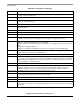
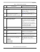
2. Use the following values for the DRAM calibration
input:
• For DDR2, connect 300 Ω 1% to GND.
• For DDR3, connect 240 Ω 1% to GND.
• For LPDDR2, connect 240 Ω 1% to GND.
• For LVDDR2, connect 300 Ω 1% to GND.
The DRAM_CALIBRATION input requires an external
resistor used as reference during DRAM output buffer
driver calibration. This resistor must be mounted close to
the associated BGA ball.