
User`s guide


Supporting the i.MX53 Camera Sensor Interface CSI0
i.MX53 System Development User’s Guide, Rev. 1
20-12 Freescale Semiconductor
interface such as the I
2
C. After the frame has been requested, the camera module takes control of the CSI
bus, and uses synchronization signals VSYNC, HSYNC, DATA_EN and PIXCLK to send the image frame
to the i.MX53. The camera sensor creates PIXCLK based on MCLK input.
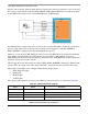
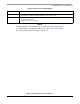
Figure 20-5. Parallel Interface Layout
In parallel interface, a single value arrives in each clock—except in BT.1120 mode when two values arrive
per cycle. Each value can be 8–16 bits wide according to the configuration of DATA_WIDTH. If
DATA_WIDTH is configured to N, then 20-N LSB bits are ignored.
Therefore, you never need CSI0_DAT[3:0], unless you are using BT.1120 mode, because the maximum
pixel width is 16 (CSI0_DAT[19:4]). The expansion port 2 includes CSI0_DAT[19:4], but only
CSI0_DAT[19:10] are used for the CSI data bus (10-bit wide data). CSI0_DAT[9:4] are shared with other
interfaces and are used for audio and I
2
C.
CSI can supports several data formats according to SENS_DATA_FORMAT configuration. When the data
format is YUV, the output of the CSI is always YUV444—even if the data arrives in YUV422 format.
The polarity of the inputs can be configured using the following registers:
• SENS_PIX_CLK_POL
•DATA_POL
•HSYNC_POL
•VSYNC_POL
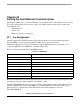
The camera parallel interface provided by the i.MX53 is a 15 line interface, as described in Table 20-3:
Table 20-3. CSI0 Parallel Interface Signals
Signal IPU Pin Description
MCLK CSI0_MCLK Master Clock (Output)
PIXCLK CSI0_PIXCLK Pixel Clock
VSYNC CSI0_VSYNC Vertical Synchronization signal
HSYNC CSI0_HSYNC Horizontal Synchronization signal