
User`s guide


Supporting the i.MX53 Camera Sensor Interface CSI0
i.MX53 System Development User’s Guide, Rev. 1
Freescale Semiconductor 20-11
For details, refer to the “Image Processing Unit (IPU)” chapter in the i.MX53 Applications Processor
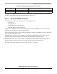
Reference Manual. Figure 20-4 shows the block diagram.
Figure 20-4. IPU Block Diagram
Several sensors can be connected to each of the CSIs. Simultaneous functionality (for sending data) is
supported as follows:
• Two sensors can send data independently, each through a different port.
• One stream can be transferred to the VDI or IC for on-the-fly processing while the other one is sent
directly to system memory.
The input rate supported by the camera port is as follows:
• Peak: up to 180 MHz (values/sec)
• Average (assuming 35% blanking overhead), for YUV 4:2:2
— Pixel in one cycle (BT.1120): up to 135 MP/sec, e.g. 9 Mpixels at 15 fps
— Pixel on two cycles (BT.656): up to 67 MP/sec, e.g. 4.5 Mpixels at 15 fps.
• On-the-fly processing may be restricted to a lower input rate.
If required, additional cameras can be connected though the USB port.
20.7.2 i.MX53 CSI Parallel Interface
The CSI obtains data from the sensor, synchronizes the data and the control signals to the IPU clock
(HSP_CLK), and transfers the data to the IC and/or SMFC.
The CSI parallel interface (shown in Figure 20-5) provides a clock output (MCLK), which is used by the
sensor as a clock input reference. The i.MX53 requests either video or still images through a different
interface between the processor and the camera module. In most cases, the interface is a synchronous serial