
User`s guide


Supporting the i.MX53 Camera Sensor Interface CSI0
i.MX53 System Development User’s Guide, Rev. 1
20-2 Freescale Semiconductor
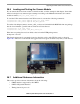
20.2 i.MX53 CSI Interfaces Layout
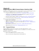
Figure 20-1 shows the camera interface layout on an i.MX53-based board.
Figure 20-1. Camera Interface Layout
Only CSI0 is used for the purpose of this document. The usage of CSI1 depends on its availability on the
board being used.
20.3 Configuring the CSI Unit in Test Mode
This chapter uses the test mode for its example scenario of a new camera driver that generates a chess
board. Setting the TEST_GEN_MODE register places the device in test mode, which is used for
debugging. The CSI generates a frame by itself and sends it to one of the destination units. The sent frame
is a chess board composed of black and configured color squares. The configured color is set with the
registers PG_B_VALUE, PG_G_VALUE and PG_R_VALUE. The data can be sent in different
frequencies according to the configuration of DIV_RATIO register.
When CSI is in test mode, configure the CSI unit with a similar configuration to the described settings in
Table 20-1. Call ipu_csi_init_interface() to configure the CSI interface protocol, formats and features.
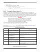
Table 20-1. Settings for Test Mode
Bit Field Value Description
CSI0_DATA_DEST 0x4 Destination is IDMAC via SMFC
CSI0_DIV_RATIO 0x0 SENSB_MCLK rate = HSP_CLK rate
CSI0_EXT_VSYNC 0x1 External VSYNC mode
CSI0_DATA_WIDTH 0x1 8 bits per color
CSI0_SENS_DATA_FORMAT 0x0 Full RGB or YUV444
CSI0_PACK_TIGHT 0x0 Each component is written as a 16 bit word where the MSB is written to
bit #15, color extension is done for the remaining least significant bits.
CSI0_SENS_PRTCL 0x1 Non-gated clock sensor timing/data mode
CSI0_SENS_PIX_CLK_POL 0x1 Pixel clock is inverted before applied to internal circuitry
CSI0_DATA_POL 0x0 Data lines are directly applied to internal circuitry.
CSI0_HSYNC_POL 0x0 HSYNC is directly applied to internal circuitry
CSI0_VSYNC_POL 0x0 VSYNC is directly applied to internal circuitry