
User`s guide


Supporting the i.MX53 Reference Board DISP0 LCD
i.MX53 System Development User’s Guide, Rev. 1
18-16 Freescale Semiconductor
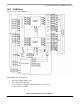
The example board’s two display interface (DI) modules are each configured to handle one or more
different kind of panels. The DI module is responsible for the timing waveforms for each signal in its
display’s interface. It is composed of the following:
• 8 sets of waveform generators (PIN1–PIN8) that control signals associated with the DI’s clock,
such as VSYNC and HSYNC.
• 12 sets of waveform generators (PIN11–PIN17 + 2 CS), controlling signals associated with data,
such as DRDY/DE, CS, or RS
The DI also generates the display’s clock based on IPU HSP_CLK or from an external clock (PLL or pin).
The IPU provides the flexibility to select from a range of pins to use as an output for the synchronization
signals. Therefore, there is no unique pin for VSYNC, HSYNC and DE. However, the i.MX51 reference
boards have been assigned a specific pin for each signal, which is reflected in the schematics and BSP
support.
To develop a system with a new LCD panel that does not have a driver already implemented, it is necessary
to implement the new driver into the Linux's kernel and do it taking the advantage of all processor's
hardware designed to the respective task, like the IPU from the i.MX53 in order to enhance the processor's
performance.
For additional details about timing and TFT signals, see AN3977, AN3978, and AN4041 (available on the
Freescale website).