
User`s guide


Avoiding Board Bring-Up Problems
i.MX53 System Development User’s Guide, Rev. 1
Freescale Semiconductor 7-3
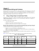
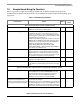
7.5 Sample Board Bring-Up Checklist
Table 7-2 provides a sample board bring-up checklist. Note that the checklist incorporates the
recommendations described in the previous sections. Blank cells should be filled in during bring-up as
appropriate.
Table 7-2. Board Bring-Up Checklist
Checklist Item Details Owner
Findings &
Status
Note: The following items must be completed serially.
1. Perform a visual inspection. Check major components to make sure nothing has been
misplaced or rotated before applying power.
2. Verify all i.MX53 voltage rails. Confirm that the voltages match the data sheet’s
requirements. Be sure to check voltages not only at the
voltage source, but also as close to the i.MX53 as possible
(like on a bypass capacitor). This reveals any IR drops on the
board that will cause issues later.
Ideally all of the i.MX53 voltage rails should be checked, but
VDDGP, VCC, and VDDA are particularly important voltages.
These are the core logic voltages and must fall within the
parameters provided in the i.MX53 data sheet.
NVCC_SRTC_POW, NVCC_XTAL, NVCC_CKIH,
NVCC_RESET, NVCC_JTAG, and NVCC_EMI_DRAM are
also critical to the i.MX53 boot up.
3. Verify power up sequence. Verify that power on reset (POR) is de-asserted (high) after
all power rails have come up and are stable. Refer to the
i.MX53 data sheet for details about power up sequencing.
This is an important process as many complex processors
are sensitive to the proper power up sequencing.
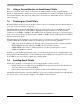
4. Measure/probe input clocks (32 kHz,
others).
Without a properly running clock, the i.MX53 will not function
properly. Look for jitter and noise.
5. Check JTAG connectivity (RV-ICE). This is one of the most fundamental and basic access points
to the i.MX53 to allow the debug and execution of low level
code.
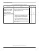
Note: The following items may be worked on in parallel with other bring up tasks.
Access internal RAM. Verify basic operation of the i.MX53 in system. The on-chip
internal RAM starts at address 0xF800_0000 and is 128
Kbytes in density. Perform a basic test by performing a
write-read-verify to the internal RAM. No software
initialization is necessary to access internal RAM.
Verify CLKO outputs (measure and
verify default clock frequencies for
desired clock output options) if the board
design supports probing of the CLKO
pin.
This ensures that the corresponding clock is working and
that the PLLs are working.
Note that this step requires chip initialization, for example via
the JTAG debugger, to properly set up the IOMUX to output
CLKO and to set up the clock control module to output the
desired clock. Refer to the reference manual for more details.