
User`s guide


Interfacing DDR2 and DDR3 Memories with the i.MX53 Processor
i.MX53 System Development User’s Guide, Rev. 1
Freescale Semiconductor 6-13
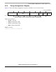
6.5.5 Timing Configuration 2 Register
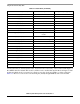
Figure 6-7 shows the timing configuration 2 register’s bit fields, access, and reset values.
Values are as follows:
• tDLLK = 512 CK
• tRTP = Greater than 4 CK
• tWTR = Greater than 4 CK
• tRRD = Greater than 4 CK
Enable as follows:
setmem /32 0x63FD9014 = 0x01FF00DB
Access: Read/Write
31 30 29 28 27 26 25 24 23 22 21 20 19 18 17 16 15 14 13 12 11 10 9 8 7 6 5 4 3 2 1 0
R
— tDLLK —tRTPtWTR tRRD
W
Reset00000000110001110000000010010010
Figure 8. ESDCTL Timing Configuration Register 2(ESDCFG2)