
User`s guide


Interfacing DDR2 and DDR3 Memories with the i.MX53 Processor
i.MX53 System Development User’s Guide, Rev. 1
6-12 Freescale Semiconductor
• tXPDLL = greater of 10 CK
• tFAW= 15 CK
•tCL=6
Enable as follows:
setmem /32 0x63FD900C = 0x555952E3
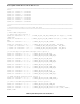
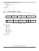
6.5.4 Timing Configuration 1 Register
Figure 6-7 shows the timing configuration 1 register’s bit fields, access, and reset values.
Values are as follows:
•tRCD = 6CK
•tRP = 6CK
• tRC = 21 CK
•tRAS = 15CK
•tRPA = tRP + 1
• tWR – 15 ns = 6CK
• tMRD = 12CK
• tCWL = 5CK
Enable as follows:
setmem /32 0x63FD9010 = 0xB68E8B63
Access: Read/Write
31 29 28 26 25 21 20 16
R
tRCD tRP tRC tRAS
W
Reset1011011010110001
15 14 12 11 9 8 5 4 3 2 0
R
tRPA — tWR tMRD — — tCWL
W
Reset1000101000100011
Figure 6-7. Timing Configuration 1 Register